This interview was originally conducted in Korean. It has been translated into English, with some expressions lightly adapted for readability.
<Section 1> Research Overview
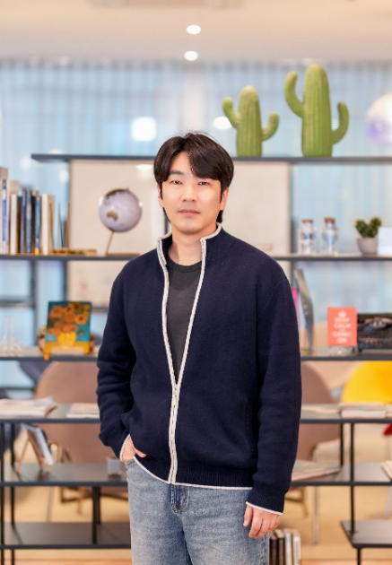
Q1. Could you briefly introduce yourself?
Hello. I am Jimin Kwon, and I joined the School of Electrical Engineering at KAIST on April 1 of this year.
I am a faculty member in the School of Electrical Engineering and also hold a joint appointment in the Department of AI Systems. I completed my bachelor’s, master’s, and doctoral studies at POSTECH. During my master’s program, I studied custom IC design, including RFIC and analog circuit design. During my doctoral program, I shifted my focus to semiconductor processes and materials. I then worked as a postdoctoral researcher on semiconductor materials in the Department of Chemical Engineering at POSTECH, followed by two years of postdoctoral research at Stanford University. After serving on the faculty at UNIST for approximately three years and eight months, I joined KAIST.
Q2. Could you explain your research areas in a way that undergraduate students can easily understand?
Our research can be broadly divided into 3D IC technology and semiconductor packaging technology. First, 3D IC technology involves vertically stacking and connecting semiconductor devices or circuits with different functions to create a single high-performance system. We develop and fabricate devices in this area while also using modeling and simulation to predict their performance when incorporated into actual integrated circuits. 3D IC research can be broadly divided into logic devices, which perform computation, and memory devices, which handle data. Our laboratory works on both areas, connecting device-level fabrication and design with IC-level performance prediction. Put simply, we do not stop at creating new semiconductor devices; we also analyze how those devices would affect the performance of an entire system when integrated into a chip.
Our second research area is semiconductor packaging. In the past, packaging primarily protected finished chips and connected them to external components. Today, advanced packaging has become a core technology that enables multiple chips to operate as a single system. To realize such multi-chip systems, our laboratory studies foundational technologies such as chip-to-chip bonding and the design, fabrication, and validation of substrate structures. We also conduct research on RF device packaging. RF devices operate at very high frequencies, and we study how to embed them in substrates and how to design and fabricate the passive components required for their operation. Our goal is to develop packaging technologies and system structures that deliver better performance at high frequencies.
Ultimately, our laboratory aims to realize new semiconductor systems in which multiple chips are efficiently connected and operated on a single substrate. Rather than limiting our work to individual devices or packages, we study the system-level benefits that emerge when multiple chips are combined, as well as the architectures best suited to such systems. Going forward, we plan to expand our research toward building complete multi-chip systems by mounting chips that we design onto substrates that we fabricate ourselves.
Q3. What differentiates your current research from conventional semiconductor research, and what new approaches does it introduce?
In 3D IC research, our distinguishing feature is that we explore new system configurations that are difficult to realize using silicon alone. Whereas conventional research has largely focused on developing silicon ICs, we investigate how emerging materials—including oxide semiconductors, two-dimensional materials, and carbon nanotubes—can be implemented as logic or memory devices and what system-level benefits they can provide when three-dimensionally integrated with silicon devices. Our approach therefore differs in that we co-design new materials, devices, and three-dimensional structures.
3D ICs are important because they can overcome interconnection limits found in conventional 2D structures. When memory and logic exist on separate chips, they must be connected through a substrate. The limited number of input/output terminals, or I/Os, can then become a system performance bottleneck. In a 3D IC, by contrast, logic and memory can be connected vertically inside the chip through vias—microscopic conductive paths that electrically connect different layers—measuring only tens of nanometers across. This allows far more connections, improves data-movement efficiency, and alleviates the memory bottleneck, in which insufficient memory bandwidth delays computation. This issue has become especially important in AI systems, including large language models, because their performance ultimately depends heavily on how much data they can retrieve and how quickly they can retrieve it. Increasing the connectivity between memory and logic through 3D IC technology can therefore make a significant contribution to improving AI system performance.
In packaging, we are also proposing structures that differ from conventional approaches. Beyond simply stacking chips on a substrate, we are investigating structures in which chips are mounted vertically, as well as new substrate structures that are advantageous for high-speed signal transmission.
In summary, our research combines new materials, devices, three-dimensional integration, and advanced packaging technologies to improve overall system performance.
Q4. What is the greatest technical bottleneck you currently face, and how are you approaching it?
The greatest technical bottleneck in 3D IC research is that multiple interdependent problems arise at the same time. A new semiconductor technology cannot be completed simply by identifying a promising material or developing a single process. Three-dimensional device integration requires the simultaneous development of processes, materials, device structures, circuit designs, and simulation environments. Even after a new device has been fabricated, an appropriate design environment is needed to build an actual circuit around it. In semiconductor design, this environment is called a process design kit, or PDK. When developing a new technology, however, the appropriate design rules and models are often not yet clearly established. Device technology and circuit design must therefore be optimized together. This approach is known as design-technology co-optimization, or DTCO.
The situation is similar in packaging research. A multi-chip module cannot be completed simply by fabricating a substrate or designing signal traces. Researchers must jointly consider how the chips will be bonded, which processes will be applied, what design constraints will arise, and how those constraints can be overcome. In packaging, this approach is called system-technology co-optimization, or STCO.
In this way, 3D IC and advanced packaging research involve a complex combination of processes, design, devices, and systems. Our laboratory therefore places great importance on interdisciplinary collaboration. Students naturally share their respective expertise, and many student-led meetings take place voluntarily. I also speak with students frequently and strive to run the laboratory in a way that enables researchers with different backgrounds to solve problems together.
In the long term, I believe that integrating AI into the research process will also be important. For problems this complex, rather than expecting a single AI system to solve everything, we will need AI agents specialized in individual domains such as processes, devices, design, and packaging. The ability of specialized AI agents and human researchers to collaborate in solving problems will become increasingly important. Although we have not yet reached the stage of implementing this vision in a concrete way, using human–AI collaboration to address complex semiconductor system challenges is one of our laboratory’s long-term goals.
Q5. In which industries or technologies could this research be applied, and what do you hope to achieve in the long term?
Our research is closely connected to the semiconductor industry as a whole. Semiconductor performance has recently become a decisive factor in the overall performance of AI systems and high-performance computing. In that sense, our work addresses technologies that are needed today while also preparing for those that will become important to the semiconductor industry in the future. We have two main technical goals: developing 3D IC technology and developing high-performance multi-chip module packaging technology. By bringing logic and memory closer together, 3D ICs can reduce bottlenecks in data movement. Multi-chip module packaging enables several chips to operate efficiently as a single system. These technologies could be applied to fields in which data movement and processing speed are critical, including AI accelerators, high-performance computing, and next-generation memory systems.
It is difficult, however, to define a single fixed long-term goal. Semiconductor technology changes extremely quickly, and the hardware required may continue to evolve with the direction of AI development. Rather than studying the same subject for ten or twenty years, I believe it is important to keep track of technological and industrial trends and identify the most pressing problem at each point in time. Many challenges also remain before commercialization. For 3D ICs, the first priority is to develop reliable devices and processes that support three-dimensional stacking. The computational methods and simulation frameworks needed to comprehensively predict 3D IC architectures and system performance are also not yet sufficiently mature. To make an industrially persuasive case, we need clear computational results and logical evidence showing what benefits new materials and devices can actually provide. Ultimately, the long-term direction of our research is to demonstrate how new semiconductor technologies can change real systems. We hope to ensure that new materials and devices, 3D ICs, and packaging technologies do not remain isolated innovations but make practical contributions to future AI systems and the semiconductor industry.
<Section 2> Experiences as a Researcher
Q1. What led you to choose your research field, and how did you make career decisions from your doctoral studies to your current position? Why did you choose to become a professor, and what career might you have pursued otherwise?
It is difficult to attribute my choice of research field to a single event. I have always tried to focus on the work in front of me and give my best effort to whatever I was doing at the time. I worked in different research areas during my master’s and doctoral studies, my postdoctoral appointments, and my career as a professor. Looking back, I believe that all of those experiences are connected and have shaped my present research direction and perspective.
I like the phrase “connecting the dots,” which Steve Jobs used in his Stanford University commencement address. It conveys the idea that the individual experiences in our lives eventually connect to shape our identity and sense of self. I feel that I have gone through a similar process. Experiences gained by focusing on the work at hand accumulate into a unique background, which then becomes the foundation of each person’s own story. For that reason, I believe it is important for students to be fully engaged in their lives, whether as undergraduates or graduate students, and to make an effort to find meaning in what they are doing.
I chose academia because I saw it as a career that would allow me to decide what I wanted to study and directly show the world the insights I had developed. I have been fortunate to encounter many opportunities and choices throughout my life, and following them seems to have brought me to where I am today. I have not seriously considered what I would have done if I had not become a professor, but I think starting a business could have been interesting. Ultimately, I believe that the purpose of technological development is to improve people’s lives, so I remain open to entrepreneurship someday. Having decided to work in engineering, I likely would have pursued one of those two paths.
Q2. Having worked at several stages of an academic career, how did your research and collaboration styles change across different environments?
As an undergraduate, I worked on internet and communications research. During my master’s program, I studied RFIC and analog IC design. I then moved into semiconductor-device processing during my doctoral studies and nanoscale processing related to materials and 3D ICs as a postdoctoral researcher. Looking back, those varied research experiences formed the background for why I pursue my current work. I was happy in each environment and was fortunate to have many positive experiences at every stage. That is why I am also very excited about my future at KAIST.
What changed most across environments was the research culture and style of collaboration. KAIST offers many opportunities to interact with faculty members from different areas. UNIST has many young researchers and a highly forward-looking atmosphere that makes it an excellent place to focus on research. At Stanford, I was particularly impressed by the culture of respect for diversity. People did not judge others hastily, and relationships between professors and students were relatively egalitarian. It was also striking that researchers had confidence that their work could change the world. Finally, POSTECH holds deep personal meaning for me because I spent so many years there. Its relatively small student body created a close-knit atmosphere in which I could have a wide variety of experiences.
Q3. Have you encountered difficulties within or beyond your research? How did you overcome them and find a way forward?
Overcoming hardship is difficult for everyone, but ultimately, sometimes you simply have to grit your teeth and push through. As experiences accumulate, you come to realize how important it is to trust yourself and protect your sense of self. Rather than allowing a challenge to consume me, I tried to step back and view myself separately from the difficulty I was facing.
I also believe that the experience of solving small problems one at a time is extremely important. As you work through problems step by step, you build trust in yourself. Eventually, difficulties that once seemed overwhelming begin to feel different and more manageable.
Q4. Students increasingly use AI for studying and research. What are your thoughts on this trend?
Ultimately, I believe every problem comes down to asking a good question. If you can formulate the right question, the path through a difficulty often becomes clearer. The most important quality when using AI is therefore an active, self-directed attitude. You should continually ask yourself what you need, what you want to understand, and how you want to grow.
This is especially important in academic study. Rather than simply completing an assigned task as if it were homework, you need to think deeply about what you genuinely want to understand. If you continue asking your own questions and searching for answers, meaningful growth will eventually follow, even if nobody recognizes it immediately.
When studying foundational subjects in electrical engineering, undergraduates may wonder what those courses have to do with their lives. Once you begin conducting research, however, you naturally realize how essential that foundational knowledge is to understanding and solving real problems. From that perspective, I hope undergraduates will try research somewhat earlier. Research provides a valuable opportunity to consider why you are studying and how you want to grow.
Q5. Of the achievements you have made throughout your research career, which moments were most rewarding or memorable? What research attitudes or approaches helped you achieve them?
There have been many moments for which I am grateful, including receiving an award at graduation, carrying out meaningful research projects, and being appointed to the faculty at KAIST. Personally, however, I feel the greatest reward when something good happens to a student who has worked with me.
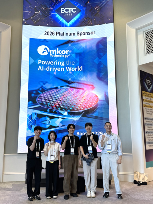
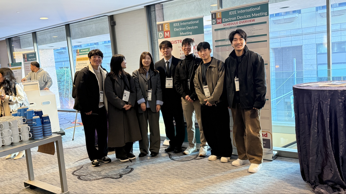
One particularly memorable moment was watching a student from my laboratory present at a major conference such as the IEEE International Electron Devices Meeting (IEDM). Seeing the student present a result that we had worked hard to achieve together was deeply moving.
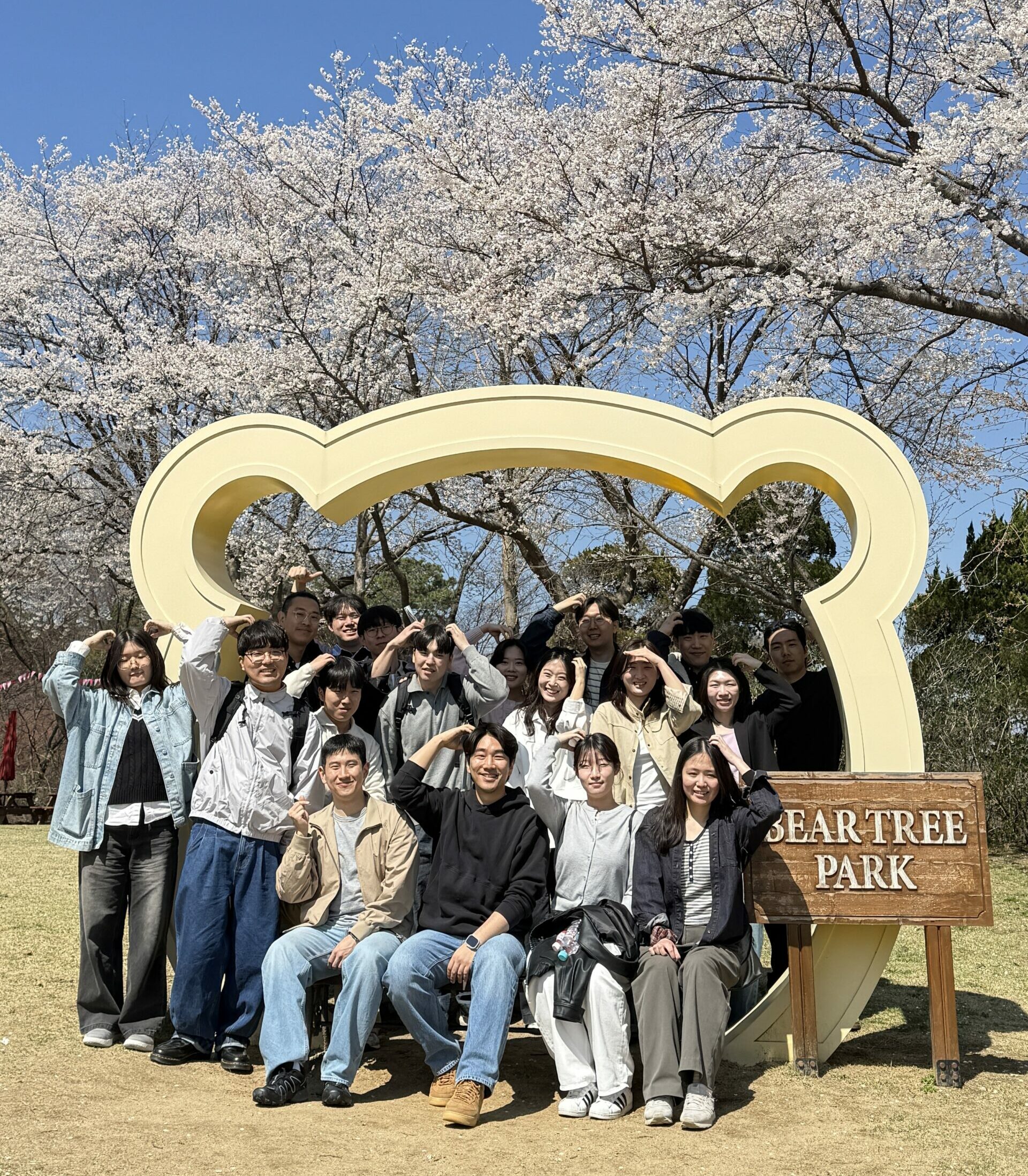
In the end, what matters most to me is seeing people thrive. I feel the greatest sense of fulfillment when students or postdoctoral researchers with whom I have worked become professors or continue to grow and succeed in their respective fields.
<Section 3> A Message to Readers

Q1. Are there any courses that prospective undergraduate or graduate researchers should take, or any qualities you particularly value when selecting students?
Because our laboratory primarily studies semiconductors, courses related to semiconductor devices, circuit design, and systems are helpful. I also value students with diverse experiences. Our laboratory brings together research from many fields, so it is important for students to find the subject they want to pursue within that environment. Studying subjects related to one’s own interests in depth can therefore be highly beneficial.
Research often brings more difficult moments than expected, so it is also important to enjoy laboratory life and maintain a positive attitude when confronting challenges.
Q2. What experiences would you recommend to undergraduate students?
I would encourage undergraduates to travel widely and experience research at least once. Fewer students than we might think have the opportunity to study and conduct research in an environment as strong as the one available here in Korea. I hope students will actively make use of the opportunities and resources around them, learn through a wide range of experiences, and fully enjoy their student years.
Q3. What qualities will researchers need in an AI-driven era of rapid change?
Ultimately, it is important to remain a thinking human being. We need the habit of asking questions and the patience to stay with a single question and think it through over time. We must also take personal responsibility for our judgments and direction. Coexistence with AI is unavoidable. Therefore, rather than merely consuming AI as a tool, we should learn to collaborate with it while pursuing ambitious work that others have not been able to accomplish.
It is also important to maintain your own center instead of being swept away by technology or temptation. Even when using technology, you must consider what meaning and direction it brings to your life. We are more easily carried along by prevailing currents than we realize. We should continually ask whether we are truly living on our own terms and avoid surrendering agency over our lives. In the spirit of Nietzsche, I believe that the determination to lead one’s own life will become even more important in the future.
Q4. Finally, is there anything you would like to say to electrical engineering students?
I hope you will look after the people around you, find happiness together, refuse to give up in the face of hardship, and preserve the individuality that makes you who you are.
Chaehun Mun, EE Newsletter Reporter — horn0122@kaist.ac.kr
Jiho Seo, EE Newsletter Reporter — ghwltj3@kaist.ac.kr