Heo, Jaehoon, et al. “SP-PIM: A Super-Pipelined Processing-In-Memory Accelerator With Local Error Prediction for Area/Energy-Efficient On-Device Learning.” IEEE Journal of Solid-State Circuits (2024).
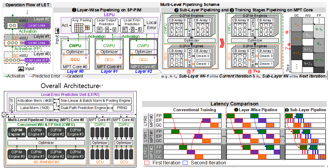
Abstract: On-device learning (ODL) is crucial for edge devices as it restores machine learning (ML) model accuracy in changing environments. However, implementing ODL on battery-limited devices faces challenges due to large intermediate data generation and frequent processor-memory data movement, causing significant power consumption. To address this, some edge ML accelerators use processing-in-memory (PIM), but they still suffer from high latency, power overheads, and incomplete handling of data sparsity during training. This paper presents SP-PIM, a high-throughput super-pipelined PIM accelerator that overcomes these limitations. SP-PIM implements multi-level pipelining based on local error prediction (EP), increasing training speed by 7.31× and reducing external memory access by 59.09%. It exploits activation and error sparsity with an optimized PIM macro. Fabricated using 28-nm CMOS technology, SP-PIM achieves a training speed of 8.81 epochs/s, showing state-of-the-art area (560.6 GFLOPS/mm²) and power efficiency (22.4 TFLOPS/W). A cycle-level simulator further demonstrates SP-PIM’s scalability and efficiency.
Main Figure

Heo, Jaehoon, et al. “PRIMO: A Full-Stack Processing-in-DRAM Emulation Framework for Machine Learning Workloads.” 2023 IEEE/ACM International Conference on Computer Aided Design (ICCAD). IEEE, 2023.
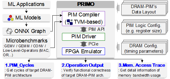
Abstract: The increasing size of deep learning models has made excessive memory access between AI processors and DRAM a major system bottleneck. Processing-in-DRAM (DRAM-PIM) offers a solution by integrating compute logic within memory, reducing external memory access. Existing simulators are often too slow for full applications, and FPGA-based emulators have been introduced, but none include the full software stack. This paper introduces PRIMO, the first full-stack DRAM-PIM emulation framework for end-to-end ML inference. PRIMO allows software developers to test ML workloads without real DRAM-PIM chips and helps designers explore design space. Our real-time FPGA emulator delivers results significantly faster than CPU-based simulations. We also provide a PIM compiler and driver to support various ML workloads with high bandwidth utilization. PRIMO achieves 106.64-6093.56× faster emulation for ML tasks compared to CPU simulations.
Main Figure

Title: A 28nm 4.96 TOPS/W End-to-End Diffusion Accelerator with Reconfigurable Hyper-Precision Unified Non-Matrix Processing Engine
Venue: ESSERC 2024
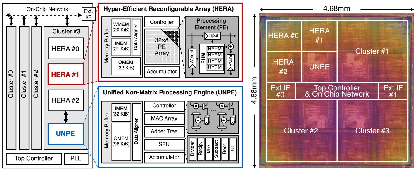
Abstract: This paper presents Picasso, an end-to-end diffusion accelerator. Picasso proposes a novel hyper-precision data type and reconfigurable architecture that can maximize hardware efficiency with extended dynamic range, with no compromise in accuracy. Picasso also proposes a unified engine operating all non-matrix operations in a streamlined processing flow and minimizes the end-to-end latency by sub-block pipeline scheduling. The accelerator is fabricated in 28nm CMOS technology and achieves an energy efficiency of 4.96 TOPS/W and a peak performance of 9.83 TOPS. Compared with prior works, Picasso achieves speedups of 8.4×-26.8× while improving energy and area efficiency by 1.1×-2.8× and 3.6×-30.5×, respectively.
Main Figure:
Prasetiyo, Adiwena Putra, and Joo-Young Kim, “Morphling: A Throughput-Maximized TFHE-based Accelerator using Transform-domain Reuse ,” IEEE HPCA 2024
Abstract:
Fully Homomorphic Encryption (FHE) has become an increasingly important aspect in modern computing, particularly in preserving privacy in cloud computing by enabling computation directly on encrypted data. Despite its potential, FHE generally poses major computational challenges, including huge computational and memory requirements. The bootstrapping operation, which is essential particularly in Torus-FHE (TFHE) scheme, involves intensive computations characterized by an enormous number of polynomial multiplications. For instance, performing a single bootstrapping at the 128-bit security level requires more than 10,000 polynomial multiplications. Our in-depth analysis reveals that domain-transform operations, i.e., Fast Fourier Transform (FFT), contribute up to 88% of these operations, which is the bottleneck of the TFHE system. To address these challenges, we propose Morphling, an accelerator architecture that combines the 2D systolic array and strategic use of transform-domain reuse in order to reduce the overhead of domain-transform in TFHE. This novel approach effectively reduces the number of required domain-transform operations by up to 83.3%, allowing more computational cores in a given die area. In addition, we optimize its microarchitecture design for end-to-end TFHE operation, such as merge-split pipelined-FFT for efficient domain-transform operation, double-pointer method for high-throughput polynomial rotation, and specialized buffer design. Furthermore, we introduce custom instructions for tiling, batching, and scheduling of multiple ciphertext operations. This facilitates software-hardware co-optimization, effectively mapping high-level applications such as XG-Boost classifier, Neural-Network, and VGG-9. As a result, Morphling, with four 2D systolic arrays and four vector units with domain transform reuse, takes 74.79 mm2 die area and 53.00 W power consumption in 28nm process. It achieves a throughput of up to 147,615 bootstrappings per second, demonstrating improvements of 3440× over the CPU, 143× over the GPU, and 14.7× over the state-of-the-art TFHE accelerator. It can run various deep learning models with sub-second latency.

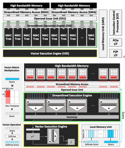
Seungjae Moon, Jung-Hoon Kim, Junsoo Kim, Seongmin Hong, Junseo Cha, Minsu Kim, Sukbin Lim, Gyubin Choi, Dongjin Seo, Jongho Kim, Hunjong Lee, Hyunjun Park, Ryeowook Ko, Soongyu Choi, Jongse Park, Jinwon Lee, and Joo-Young Kim, “LPU: A Latency-Optimized and Highly Scalable Processor for Large Language Model Inference,” IEEE Micro, Sep. 2024
Abstract: The explosive arrival of OpenAI’s ChatGPT has fueled the globalization of large language model (LLM), which consists of billions of pretrained parameters that embodies the aspects of syntax and semantics. HyperAccel introduces latency processing unit (LPU), a latency-optimized and highly scalable processor architecture for the acceleration of LLM inference. LPU perfectly balances the memory bandwidth and compute logic with streamlined dataflow to maximize performance and efficiency. LPU is equipped with expandable synchronization link (ESL) that hides data synchronization latency between multiple LPUs. HyperDex complements LPU as an intuitive software framework to run LLM applications. LPU achieves 1.25 ms/token and 20.9 ms/token for 1.3B and 66B model, respectively, which is 2.09x and 1.37x faster than the GPU. LPU, synthesized using Samsung 4nm process, has total area of 0.824 mm2 and power consumption of 284.31 mW. LPU-based servers achieve 1.33x and 1.32x energy efficiency over NVIDIA H100 and L4 servers, respectively.
Main figure
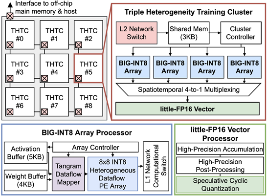
Title: JNPU: A 1.04TFLOPS Joint-DNN Training Processor with Speculative Cyclic Quantization and Triple Heterogeneity on Microarchitecture / Precision / Dataflow
Venue: ESSCIRC 23
Abstract: This paper presents JNPU, a 1.04TFLOPS joint- DNN accelerator that can simultaneously run joint-DNN (MobileNet + GoogLeNet) models with 245FPS (inference) and 1.26TFLOPS/W (training). It proposes speculative cyclic quantization that enables integer-dominant operations and reduces external memory access by 87.5%. Its tangram dataflow mapper provides optimized sets of heterogeneous stationary types for both forward and backward propagation, enhancing efficiency up to 71.6%. Lastly, its novel processing cluster leverages triple heterogeneity on INT8 arrays and FP16 vector processor, saving 56.3% and 26.9% of computing area and power, respectively.
Main Figure:
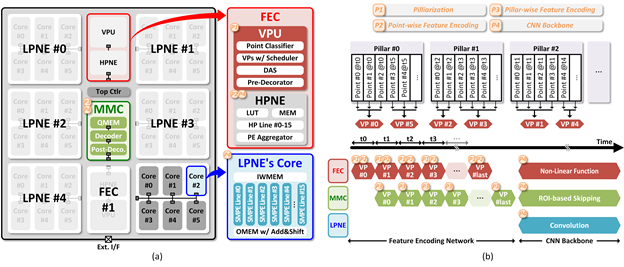
Title: A 38.5TOPS/W Point Cloud Neural Network Processor with Virtual Pillar and Quadtree-based Workload Management for Real-Time Outdoor BEV Detection
Venue: CICC 2024
Abstract: A large-scale 3D processing using point cloud neural network (PNN) has become essential for applications such as autonomous driving system. Among the various methods, pillarbased PNN is widely utilized for processing large-scale outdoor environment. However, due to the irregular and sparse nature of point cloud compared to the regular and dense image, achieving high efficiency has been challenging in previous works. Inspired by the LiDAR mechanism that generates point cloud, this article proposes Hawkeye, a large-scale bird’s-eye-view (BEV) detection processor designed for end-to-end processing of pillar-based PNN. Hawkeye incorporates three key features: 1) a feature encoding core (FEC) that introduces virtual pillars, dynamically generating temporal pillars to facilitate continuous processing; 2) a map management core (MMC) that utilizes a quadtree-based workload management system, enabling region-of-interest (ROI)- based skipping to optimize computational efficiency; and 3) a lowprecision neural engine (LPNE) that employs a bit-slice compute architecture with sign-magnitude (SM) representation, enhancing slice-level skipping (SLS) capabilities. Fabricated in Samsung’s 28nm CMOS technology, Hawkeye achieves a performance of 44.2 frames per second (FPS) at 320MHz on the PointPillars with the KITTI dataset. Furthermore, with the aid of ROI-based skipping and SM-based SLS, Hawkeye demonstrates an effective energy efficiency of 38.5 TOPS/W under 0.74V and 40MHz.
Main Figure:
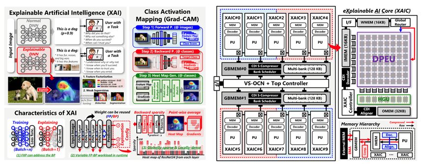
Title: A 26.55TOPS/W Explainable AI Processor with Dynamic Workload Allocation and Heat Map Compression/Pruning
Venue: 2023 IEEE Custom Integrated Circuits Conference (CICC)
Abstract: Explainable AI aims to provide a clear and human-understandable explanation of the model’s decision, thereby building more reliable systems. However, the explanation task differs from well-known inference and training processes as it involves interactions with the user. Consequently, existing inference and training accelerators face inefficiencies when processing explainable AI on edge devices. This paper introduces explainable processing unit (EPU), the first hardware accelerator designed for explainable AI workloads. The EPU utilizes a novel data compression format for the output heat maps and intermediate gradients to enhance the overall system performance by reducing both memory footprint and external memory access. Its sparsity-free computing core efficiently handles the input sparsity with negligible control overhead, resulting in a throughput boost of up to 9.48x. It also proposes a dynamic workload scheduling with a customized on-chip network for distinct inference and explanation tasks to maximize internal data reuse hence reducing external memory access by 63.7%. Furthermore, the EPU incorporates point-wise gradient pruning that can significantly reduce the size of heat maps by a factor of 7.01x combined with the proposed compression format. Finally, the EPU chip fabricated in a 28nm CMOS process achieves the state-of-the-art area and energy efficiency of 112.3 GOPS/mm2 and 26.55 TOPS/W, respectively.
Main Figure: 
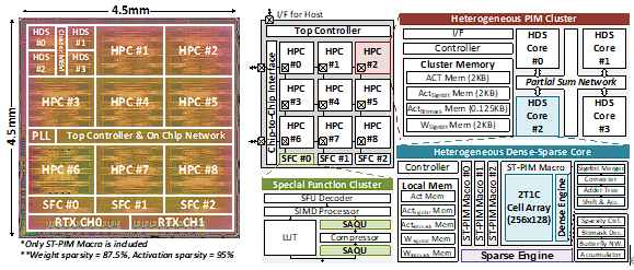
Donghyuk Kim, Jae-Young Kim, Hyunjun Cho, Seungjae Yoo, Sukjin Lee, Sungwoong Yune, Hoichang Jeong, Keonhee Park, Ki-Soo Lee, Jongchan Lee, Chanheum Han, Gunmo Koo, Yuli Han, Jaejin Kim, Jaemin Kim, Kyuho Lee, Joo-Hyung Chae, Kunhee Cho, and Joo-Young Kim, “DPIM: A 19.36 TOPS/W 2T1C eDRAM Transformer-in-Memory Chip with Sparsity-Aware Quantization and Heterogeneous Dense-Sparse Core,” IEEE European Solid-State Electronics Research Conference, Sep. 2024
Abstract: This paper presents DPIM, the first 2T1C eDRAM Transformer-in-memory chip. Its high-density eDRAM cell supports large-capacity processing-in-memory (PIM) macros of 1.38 Mb/mm2, reducing external memory access. DPIM adopts a sparse-aware quantization scheme to entire layers of Transformer, which quantizes the model to 8-bit integer (INT8) with a minimal accuracy drop of 2\% in the BERT-large model on the GLUE dataset while increasing the bit-slice sparsity ratio of both weight and activation from dense matrices to 83.3\% and 88.4\%, respectively. Its heterogeneous PIM macro supports intensive dense matrix multiplications with an extreme to moderate range of sparse matrix multiplications with a peak throughput of 3.03-12.12 TOPS, enhancing the efficiency up to 4.84-19.36 TOPS/W.
Main figure
Title: APINT: A Full-Stack Framework for Acceleration of Privacy-Preserving Inference of Transformers based on Garbled Circuits
Venue: ICCAD 2024
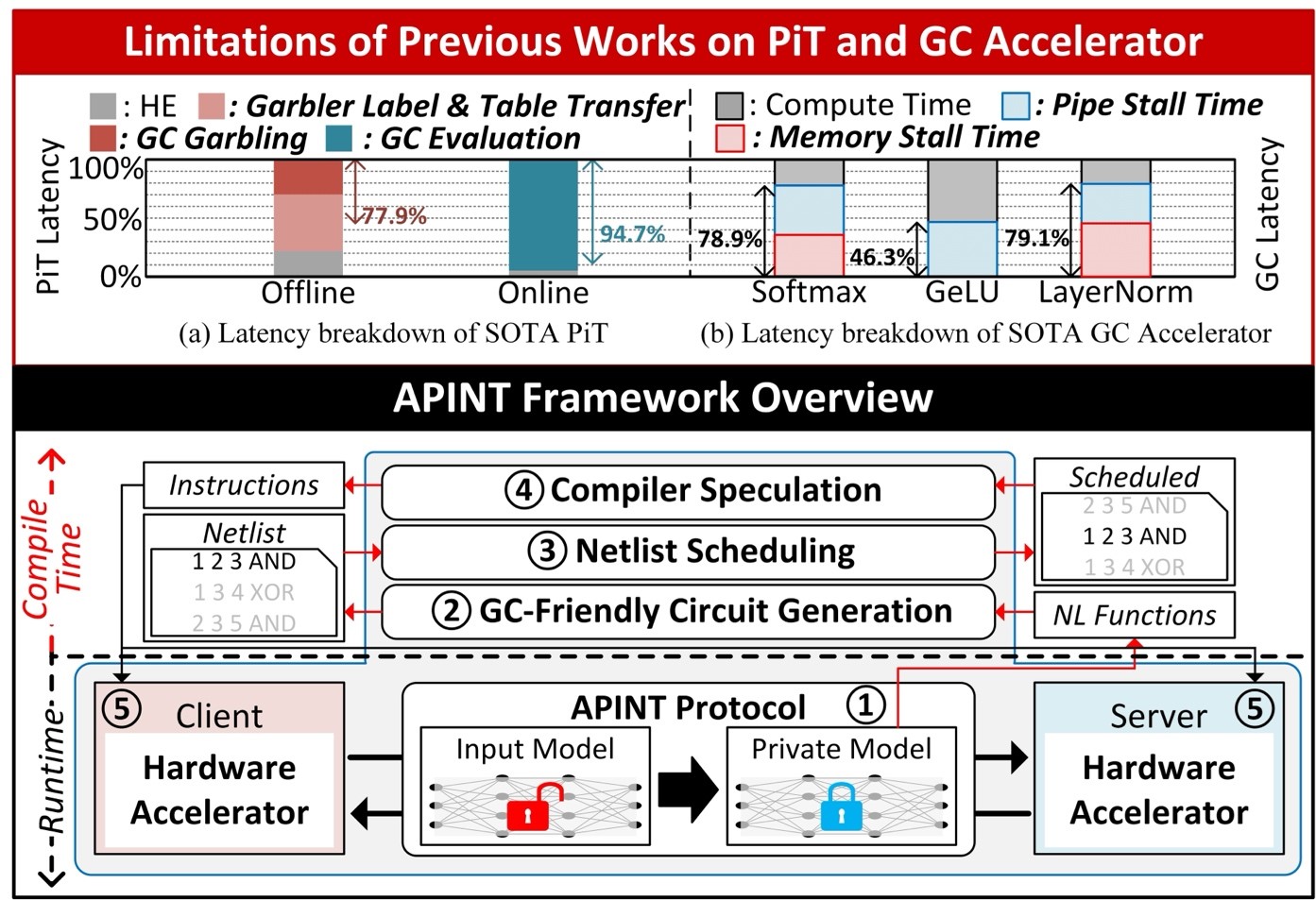
Abstract: This paper introduces APINT, the first full-stack framework to accelerate Private Inference of Transformers (PiT), a key solution to AI security challenges in cloud environments. It identifies garbled circuits (GC) as the main bottleneck in recent PiT protocols and provides a comprehensive solution, including a novel PiT protocol, GC-friendly circuit generation, netlist scheduling, and a hardware accelerator with compiler speculation to reduce latency and energy consumption. APINT achieves significant latency reductions, outperforming existing CPU-based platforms by 12.2× online and 2.2× in preprocessing. Meanwhile, the APINT accelerator further improves latency by 3.3× and reduces energy consumption by 4.6× compared to the state-of-the-art GC accelerator.
Main Figure: