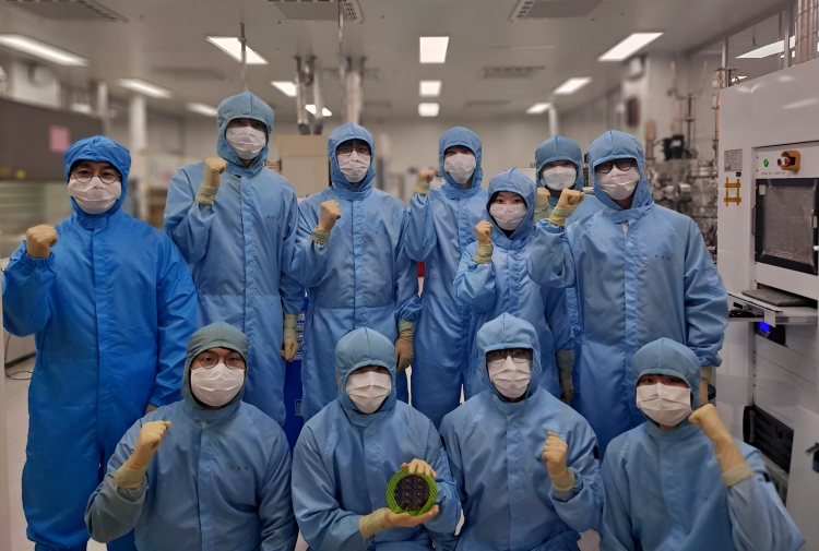
Ferroelectric materials are being highlighted as a key material for the development of next-generation semiconductor technologies due to their characteristic of storing charges well, making them comparable to a “material that remembers electricity.” The KAIST research team has succeeded in developing high-performance, high-density next-generation memory devices that overcome the limitations of DRAM and NAND Flash memory, the two pillars of the current memory semiconductor industry.
EE Professor Sanghun Jeon’s research team has developed next-generation memory and storage memory technology using hafnia-based ferroelectric materials*. *Hafnia-Based Ferroelectric Material: A non-volatile insulating material actively researched as a core material for next-generation semiconductors, with excellent physical properties such as compatibility with CMOS processes, high speed, and durability.
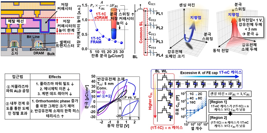
DRAM memory is a type of volatile memory used to store data in devices such as smartphones, computers, and USB drives. Because of its volatile nature, stored data is lost when external power is cut off. However, it has been used as the main memory due to its low manufacturing cost and high integration density. Despite these advantages, as DRAM memory technology advances, the size of memory cells becomes smaller, reducing the capacity of the storage capacitors that store information. This eventually makes it difficult to sustain memory operation.
The research team focused on overcoming the limitations of these storage capacitors to achieve higher storage capacity in physically small areas. To this end, they developed a hafnia-based ferroelectric ultrathin high-k material. The results showed the lowest reported equivalent oxide thickness (EOT) of 2.4 Å (approximately one ten-thousandth the thickness of a human hair) for DRAM capacitors to date.
The team also developed ferroelectric memory (FRAM), which is being considered as a potential replacement for DRAM. This technology ensures non-volatile data storage and erasure even at low voltages below 1V, significantly improving energy efficiency and making it essential for next-generation memory.
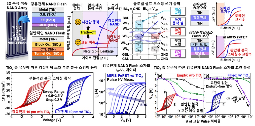
Following advancements in DRAM technology, the team developed next-generation memory technology to overcome the limitations of NAND Flash memory using hafnia-based ferroelectric materials. NAND Flash memory, a non-volatile memory used in devices like smartphones, computers, and USB drives, has evolved to increase storage capacity by stacking multiple layers. However, physical limitations make it challenging to stack more than 500 or 1,000 layers.

In response, the research team applied ferroelectric materials to NAND Flash memory, adding a thin TiO2 interfacial layer to achieve stable data retention in a 3D vertical structure with over 1,000 layers. Furthermore, the team succeeded in developing a high-performance oxide channel-based NAND Flash device, capable of storing more data and maintaining data stability for over 10 years, overcoming the limitations of traditional oxide channel-based memory devices that struggled with complete data erasure.
Professor Jeon stated, “These research results are expected to provide a breakthrough in memory semiconductor technology, which has been stagnant due to scaling issues, and contribute to the commercialization of various AI computing and edge computing technologies in the future.”

Dr. Venkateswarlu Gaddam, PhD candidates Ki-Wook Kim, Hong-Rae Cho, Jung-Hyun Hwang, Sang-Ho Lee, master’s students Hyo-Jun Choi and Hyun-Jun Kang participated as co-first authors. These research achievements were internationally recognized, with five papers presented at top-tier semiconductor industry conferences in 2024 (2 at VLSI 2024, 3 at IEDM 2024).
- “In-depth analysis of the Hafnia ferroelectrics as a key enabler for low voltage & QLC 3D VNAND beyond 1K layers: Experimental demonstration and modeling,” VLSI 2024. DOI: 10.1109/VLSITechnologyandCir46783.2024
- “Low-Damage Processed and High-Pressure Annealed High-k Hafnium Zirconium Oxide Capacitors near Morphotropic Phase Boundary with Record-Low EOT of 2.4 Å & high-k of 70 for DRAM,” VLSI 2024. DOI: 10.1109/VLSITechnologyandCir46783.2024
- “Unveiling the Origin of Disturbance in FeFET and the Potential of Multifunctional TiO2 as a Breakthrough for Disturb-free 3D NAND Cell: Experimental and Modeling,” IEDM 2024.
- “Oxide Channel Ferroelectric NAND Device with Source-Tied Covering Metal Structure: Wide Memory Window (14.3 V), Reliable Retention (> 10 years) and Disturbance Immunity (△Vth ≤ 0.1 V) for QLC Operation,” IEDM 2024.
- “Design Methodology for Low-Voltage Operational (≤1 V) FRAM Cell Capacitors and Approaches for Overcoming Disturb Issues in 1T-nC Arrays: Experimental & Modeling,” IEDM 2024.
IEEE VLSI and IEEE IEDM conferences are considered the “Olympics of semiconductors,” where leading companies like Samsung Electronics, SK Hynix, Micron, and Intel, as well as renowned academics, share the latest technological advancements and discuss future directions.
This research was conducted in collaboration with Samsung Electronics and Hanyang University, supported by the Korea Evaluation Institute of Industrial Technology (KEIT), the Ministry of Science and ICT’s Innovation Research Center (IRC) program, and funding from Samsung Electronics.