Title: “Machine Learning based Optimal Signal Integrity/Power Integrity Design for 3D ICs,” is published on IEEE Trans. VLSI Systems. (https://ieeexplore.ieee.org/abstract/document/7850943)
Author: Sung-Joo Park ; Bum-Hee Bae ; Joung-Ho Kim ; Madhavan Swaminathan
Article contents
Machine Learning based Optimal Signal Integrity/Power Integrity Design for 3D ICs
1. Deep Neural Network (DNN)-based Signal integrity/Power integrity Results Estimation Method

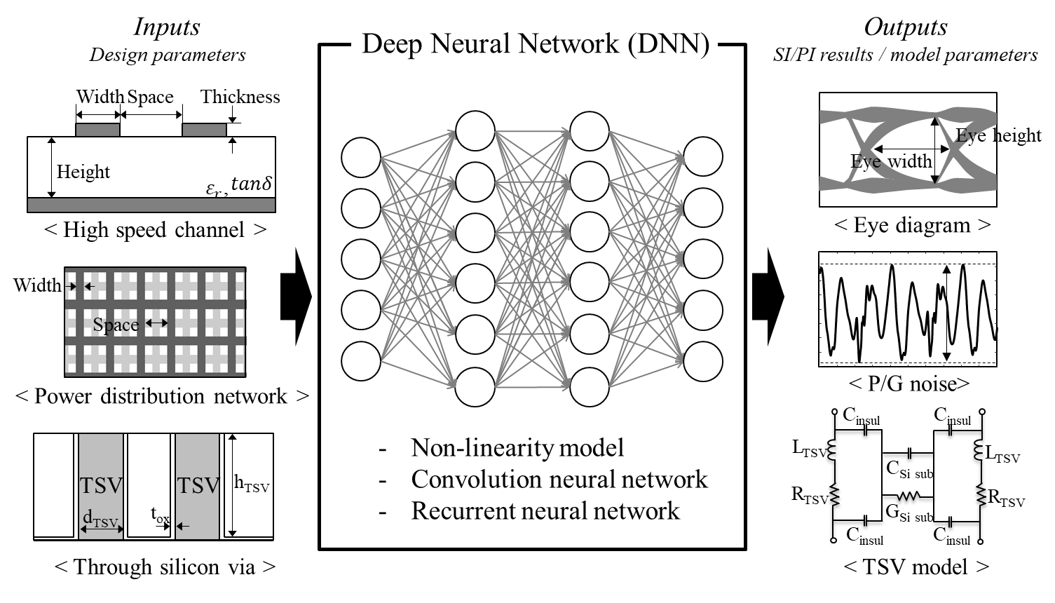
Fig. 1. Deep Neural Network (DNN)-based SI/PI results estimation method
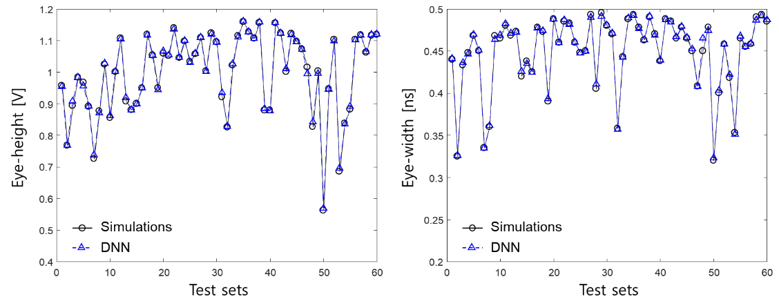
High-speed channels and power distribution networks (PDNs) must be simulated to ensure signal/power integrity in the early stage of the entire design process for the reduction of the time and cost. However, the time to simulate the entire channels and PDNs by conventional EM, circuit simulators has been longer as the complexity of the design is increased. The estimation of the SI/PI results and model parameters using the deep neural network (DNN) can save time and cost than the conventional simulations. Because the DNN can automatically solve the non-linearity relationship between input and output, DNN can accurately estimate/model the electrical characteristics of design parameters such as high speed channels, power distribution networks, and through silicon vias (TSVs) to obtain outputs such as eye diagram, P/G noise and TSV models as shown Fig. 1. Fig. 2 shows the comparison between simulation and DNN which estimate the eye height and eye width of the high speed memory channel in HBM interposer. The estimation using DNN is accurate. As a result, the DNN can be used in many ways in the SI/PI field.

Fig. 2. Comparison between simulation and DNN model which estimate the eye height and eye width.
2. Reinforcement Learning-based Signal Integrity/Power Integrity Design Method

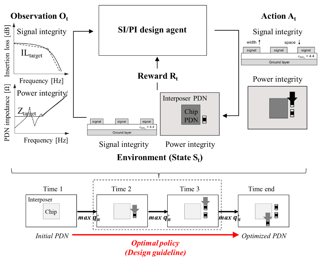
Fig. 3. Reinforcement learning (RL)-based optimal SI/PI design method.
As the demand on higher performance such as channel speed, bandwidth, and low power is increasing, the complexity of the 2.5-D/3D IC design is gradually increasing to ensure the signal/power integrity. Moreover, time-to-market is getting shorter in order to respond quickly to market trends and customer needs. Therefore, time-efficient and accurate optimal 2.5D/3D IC design is necessary in these days. Optimal layout design considering SI/PI can be performed by reinforcement learning (RL) as shown in Fig. 3.
By using RL algorithms, optimal layout design guideline which is optimal policy can be learned through reward (feedback) mechanisms depending on the target specifications of SI/PI. Therefore, high speed channels and power distribution networks (PDNs) can be designed through the RL-based optimal design method. Fig. 4 shows the results of the RL-based optimal decoupling capacitor design method. As shown in Fig. 4, the self PDN impedance of optimized PDN satisfied the target impedance and simultaneous switching noise (SSN) is suppressed.

Fig. 4. PDN self impedance and simultaneous switching noise (SSN) of the optimized PDN by the RL-based optimal design method.