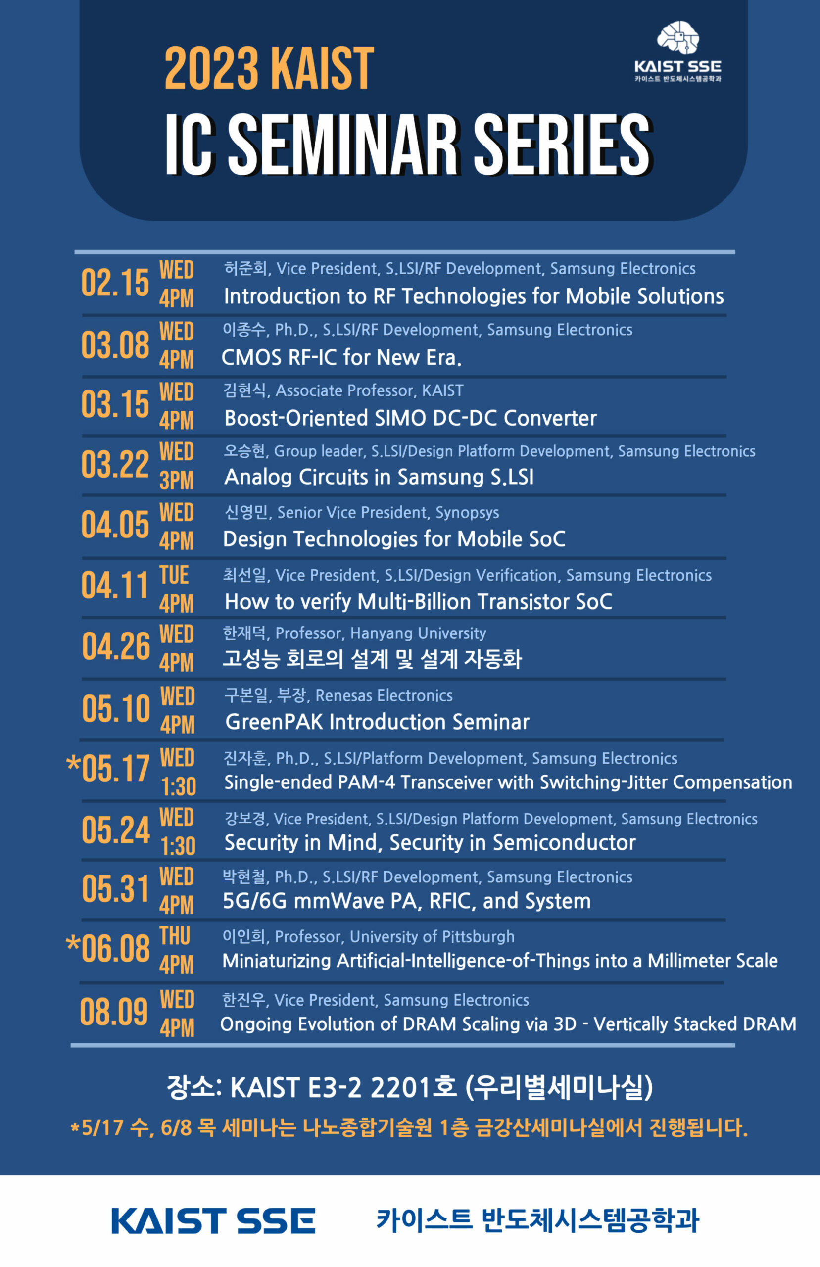
Abstract:
For the past decades, the density of DRAM has been remarkably increased by making access transistors and capacitors smaller in size per unit area. However, shrinking devices far beyond the 10 nm process node increasingly poses process and reliability challenges. As Flash technology made a pivotal and successful innovation via 3D NAND, DRAM technology may also adopt vertical stacking memory cells. Vertically stacked DRAM (VS-DRAM) continues to increase bit density on a die by increasing the number of layers along with reducing the size of the transistor. In this seminar, the opportunities and challenges of VS-DRAM are discussed.
Biography:
Jin-Woo Han is a VP of Samsung R&D Center. Since 2022, he has been leading a semiconductor research team responsible for developing novel architecture reserach team. In 2010-2022, he had been with NASA Ames Research Center for developing exploratory transistor, memory, and sensors. He has received various awards including the NASA Ames Honor Award, the IEEE Electron Device Society Early Career Award, Outstanding Engineering Achievement Merit Award from Engineers’ Council, Mike Sargeant Award from the Institute of Engineering and Technology (IET, UK), IEEE Nanotechnology Council Early Career Award and the Presidential Early Career Award for Scientists and Engineers (PECASE) Award, and served as IEEE NTC Distingushed Lectuerer. He has published over 140 articles in peer-reviewed journals and given 40 invited talks on his subject areas in international conferences and universities. He received Ph.D in EE, KAIST, 2010.
