Prof. Sung-Yool Choi & Sung Gap Im’s research group were reported in Yonhapnews, and 17 media, about the nonvolatile two-dimentional memory on December 18th, 2017.
In this research, the highly integrated, ultra-low-power, and flexible nonvolatile memory was demonstrated using two-dimensional material (MoS2) and polymer insulating thinfilm.
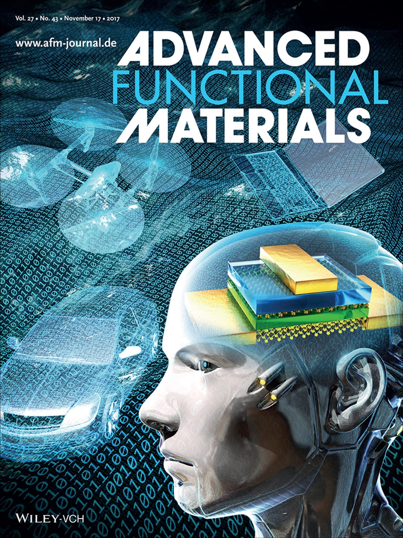
The study was published as a cover paper in November 2017 in the international journal ‘Advanced Functional Materials’. (Impact factor 2017: 12.12)
Media: ‘KAIST, implement a ultra-low-power flexible memory‘
https://www.yna.co.kr/view/AKR20171218056900063?input=1195m
KAIST News: ‘Ultra-Low Power Flexible Memory Using 2D Materials’
https://www.kaist.ac.kr/_prog/_board/?mode=V&no=75023&code=ed_news&site_dvs_cd=en&menu_dvs_cd=060101&list_typ=B&skey=&sval=&smonth=&site_dvs=&GotoPage=11
Article title: Low‐Power Nonvolatile Charge Storage Memory Based on MoS2 and an Ultrathin Polymer Tunneling Dielectric
A research article authored by Myung Hun Woo (KAIST EE), Byung Chul Jang (KAIST EE), Junhwan Choi (KAIST CBE), Khang June Lee (KAIST EE), Gwang Hyuk Shin (KAIST EE), Hyejeong Seong (KAIST CBE), Sung Gap Im (KAIST CBE), and Sung‐Yool Choi (KAIST EE; Corresponding author) was published at Advanced Functional Materials (2017.11)
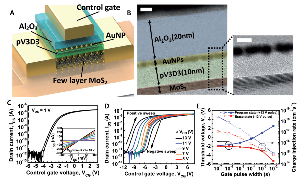
Low-power, nonvolatile memory is an essential electronic component to store and process the unprecedented data flood arising from the oncoming Internet of Things era. Molybdenum disulfide (MoS2) is a 2D material that is increasingly regarded as a promising semiconductor material in electronic device applications because of its unique physical characteristics. However, dielectric formation of an ultrathin low-k tunneling on the dangling bond-free surface of MoS2 is a challenging task. Here, MoS2-based low-power nonvolatile charge storage memory devices are reported with a poly(1,3,5-trimethyl- 1,3,5-trivinyl cyclotrisiloxane) (pV3D3) tunneling dielectric layer formed via a solvent-free initiated chemical vapor deposition (iCVD) process. The surface-growing polymerization and low-temperature nature of the iCVD process enable the conformal growing of low-k (≈2.2) pV3D3 insulating films on MoS2. The fabricated memory devices exhibit a tunable memory window with high on/off ratio (≈106), excellent retention times of 105 s with an extrapolated time of possibly years, and an excellent cycling endurance of more than 103 cycles, which are much higher than those reported previously for MoS2-based memory devices. By leveraging the inherent flexibility of both MoS2 and polymer dielectric films, this research presents an important milestone in the development of low-power flexible nonvolatile memory devices.

Figure 1. A Schematic illustration of the fabricated memory device, which is composed of a pV3D3 tunneling dielectric, AuNPs as floating gate, and an Al2O3 blocking dielectric layer. B Cross-sectional TEM image of the device. C Initial transfer characteristics of the memory device with control gate voltage. The inset shows the memory device contact properties. D Transfer characteristics with VCG sweeping in the negative-to-positive direction and back, with fixed VDS = 1 V. E Extracted threshold voltage shift for different pulse widths, and calculated charge injection rate in program and erase operations.
