A research article authored by Jae Hur (KAIST EE), Byung Chul Jang (KAIST EE), Jihun Park (KAIST EE), Dong-Il Moon (KAIST EE), Hagyoul Bae (KAIST EE), Jun-Young Park (KAIST EE), Gun-Hee Kim (KAIST EE), Seung-Bae Jeon (KAIST EE), Myungsoo Seo (KAIST EE), Sungho Kim (KAIST EE), Sung-Yool Choi (KAIST EE; Corresponding author), and Yang-Kyu Choi (KAIST EE; Corresponding author) was published at Advanced Functional Materials (2018.11)
Article title: A Recoverable Synapse Device Using a Three-Dimensional Silicon Transistor
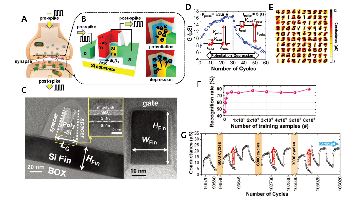
To prepare for the upcoming big-data era, numerous attempts are underway to develop a neuromorphic system which is capable of imitating a biologic neural network. Despite the significant improvements to software-based artificial neural networks (ANNs) recently, they remain inefficient in terms of energy use. Alternatively, many researchers have been attracted to hardware-based ANNs by fundamentally mimicking neural circuits and synapses. In this study, a two-terminal silicon-channel synapse (SINAPSE) with a poly-Si/SiO2/Si3N4 gate stack over a silicon channel is introduced, and demonstrated the smallest size of a synapse device reported thus far, along with reliable, low-power performance. A distinctive feature of SINAPSE is that it emulates synaptic recovery, a retrieval process for neurotransmitters which would be otherwise depleted. By applying an electrical recovery pulse to SINAPSE, synaptic recovery was for the first time successfully imitated. Experimental results demonstrate the potential of the curable SINAPSE as a fundamental unit in neuromorphic circuitry.

Figure 1. A A schematic illustration of a synapse between a presynaptic and postsynaptic neuron in a biological system. B A schematic of the SINAPSE structure and the electron trajectories during the potentiation and depression processes of the charge-trap nitride of SINAPSE. C Cross-sectional TEM images of SINAPSE along the silicon nanowire direction (left-side panel) and along the gate direction (right-side panel). D Analog conductance modulation behavior of SINAPSE as a function of the number of applied pulse cycles. (Inset) Applied presynaptic voltage schemes for potentiation and depression. E Learned weights map with the ANN, which is based on a SINAPSE device with 100 output neurons. F Recognition rate as a function of the number of the number of training instances. G Recovery (Vpulse = 6 V and tpulse = 1 ms) results for SINAPSE after fatigue.