“A Stamp Of Approval For Graphene Transfer” from Asian Scientist Magazine

Asian Scientist (Jan. 30, 2015) – Researchers have developed a new technique to produce a single-layer graphene from a metal etching. The research findings, published as the lead article in the journal Small, mean that transferring a graphene layer onto a circuit board can be done as easily as stamping a seal on paper.
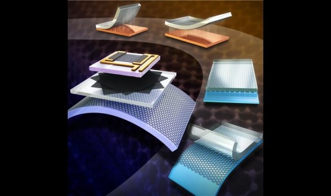
This technology will allow different types of wafer transfer methods such as transfer onto a surface of a device or a curved surface and large surface transfer onto a four inch wafer. It can be applied in the field of wearable smart gadgets through commercialization of graphene electronic devices.
The traditional method used to transfer graphene onto a circuit board is a wet transfer. However, wet transfer faces serious drawbacks as the graphene layer can be damaged or contaminated during the transfer process from residue from the metal etching. This may affect the electrical properties of the transferred graphene.
Instead, a team of researchers led by Professor Choi Sung-Yool from the Korea Advanced Institute of Science and Technology (KAIST) have adopted a stamping approach. After a graphene growth substrate formed on a catalytic metal substrate is pretreated in an aqueous poly vinyl alcohol (PVA) solution, a PVA film forms on the pretreated substrate. The substrate and the graphene layers bond strongly. The graphene is then lifted from the growth substrate by means of an elastomeric stamp.
The delaminated graphene layer is isolated state from the elastomeric stamp and thus can be freely transferred onto a circuit board. As the catalytic metal substrate can be reused and does not contain harmful chemical substances, such transfer method is very eco-friendly.
“As the new graphene transfer method has a wide range of applications and allows a large surface transfer, it will contribute to the commercialization of graphene electronic devices,” Choi said.
He added that “because this technique has a high degree of freedom in transfer process, it has a variety of usages for graphene and two dimensional nano-devices.”
The article can be found at:
Yang et al. (2015) Metal-Etching-Free Direct Delamination and Transfer of Single-Layer Graphene with a High Degree of Freedom
http://onlinelibrary.wiley.com/doi/10.1002/smll.201401196/abstract