Professor Lee Kayoung’s research team develops Superior Electron Mobility and Electron Saturation Velocity Characteristics of the New Device Compared to Existing Devices

<(from left) Professor Kayoung Lee, Yongwook Seok ph.d candidate>
Professor Lee Kayoung’s research team has successfully developed a high-performance 2D semiconductor device that can operate at ultra-high speeds and whose performance improves as the temperature decreases, showing potential for use in high-frequency bands and at extremely low temperatures.
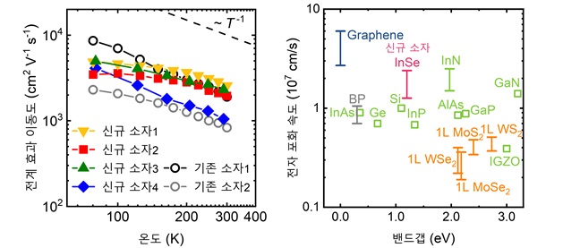
The research team led by Professor Lee Kayoung announced on the 20th that they have developed a high-mobility, ultra-high-speed device based on two-dimensional nano-semiconductor indium selenide (InSe), which surpasses the electron mobility and saturation velocity of silicon by more than two-fold.
*Saturation velocity: Refers to the maximum speed at which electrons or holes can move within a semiconductor material. Saturation velocity is a key indicator for evaluating the electrical properties of a semiconductor, as it determines saturation current and cutoff frequency, among other factors.
**Indium Selenide (InSe): An inorganic compound made of indium and selenium that forms two-dimensional layers with van der Waals bonds.
Two-dimensional indium selenide is attracting attention as a next-generation semiconductor material due to its higher electron mobility and current compared to traditional silicon semiconductors and 2D semiconductors. However, indium selenide is vulnerable to oxidation in the air and has lower stability, making the development of high-performance devices challenging.
Professor Lee Kayoung’s research team improved the stability and performance of indium selenide by using high-quality two-dimensional hexagonal boron nitride (hBN) as the lower insulating layer and thin indium metal as the upper protective layer to solve this problem.
*Hexagonal Boron Nitride (hBN): Nitrogen and boron form a hexagonal planar structure and have insulating properties.
Additionally, by forming a two-dimensional heterojunction* structure without contaminating the core channel layer of indium selenide, they significantly improved the electron mobility and electron saturation velocity. This is the first time that the electron saturation velocity of indium selenide has been systematically analyzed, and the research team was able to determine the mechanism for electron saturation velocity.
*Heterojunction: The interface between two layers or regions of different crystalline semiconductors

< Figure 1. Superior Electron Mobility and Electron Saturation Velocity Characteristics of the New Device Compared to Existing Devices >
Leading this research, doctoral candidate Seok Yongwook said, “Through the development of high-performance devices, we were able to confirm the high electron mobility and saturation velocity of the two-dimensional semiconductor indium selenide,” and added, “Research on its application is necessary for actual devices that require ultra-low temperature and high-frequency operation.”
Professor Lee Kayoung said, “The high-performance electronic device developed this time is capable of ultra-fast operation, making it possible to operate in the 6G frequency band beyond the 5G band,” and “As the temperature decreases, the performance of the device improves significantly, making it suitable for ultra-low temperature high-frequency operation environments like those needed for quantum computer quantum control ICs (Integrated Circuits).”
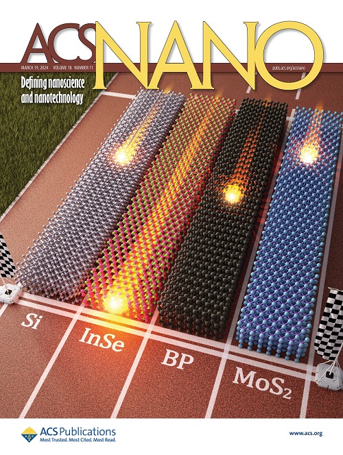
This research, with doctoral student Seok Yongwook from the Department of Electrical and Electronic Engineering as the lead author, was officially published in the international journal of nanoscience, `ACS Nano (Nano),’ on March 19, 2024, and was also featured as the journal cover article. (Paper title: High-Field Electron Transport and High Saturation Velocity in Multilayer Indium Selenide Transistors)
Meanwhile, this research was conducted with the support of the National Research Foundation of Korea’s Young Researchers Program, Basic Research Program, BK21, KAIST’s C2 (Creative & Challenging) Project, LX Semicon-KAIST Future Technology Center, and the Posco Foundation.
< Figure 2. Cover Image of the ACS Nano Journal >


