Research
Research Centers

Website
Research
Area
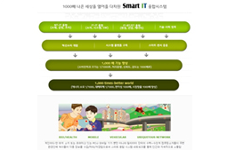
Development of innovative devices, circuits, element technology and system technology to overcome the stagnation in the growth of IT
Development of common platforms with various devices and sensors
Creation of epoch-making ‘Multi-dimensional Smart IT Convergence Systems’ with more than 1,000 times improved Figure of Merits in terms of information processing speed, energy, and physical volume based on the optimization of platform performances through the convergence of hardware and software technologies

Website
Research
Area
Personal Plug&Play DigiCar Platform
Distributed Embedded Computing Platform supporting plug and play
Driver- Assistant Active Safety System
Distributed Embedded Computing Platform supporting plug and play
Driver- Assistant Active Safety System

Website
Research
Area
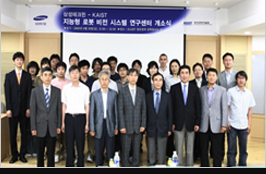
Joint research and cooperation for developing intelligent robot technology, such as robot control, vision, artificial intelligence, wireless communication, sensing.
Development of technologies for multi-sensor fusion based robot localization and scene understanding on static camera.
Development of technologies for vision sensor based robot localization and scene understanding on moving camera.
Development of technologies for environment understanding on mobile robot and high resolution camera.
Development of technology for multi-camera object tracking.

Website
Research
Area
Development of a body-brain convertible PET system and a 3D breast ultrasound imaging system

Website
Location
Research
Area
Server power supply with high efficiency and high power density for a data center
Digital control for the power supply of OLED, LED backlight TV
Advanced power system and power converter for a next generation
Digital control for the power supply of OLED, LED backlight TV
Advanced power system and power converter for a next generation

Website
Location
Research
Area
Provide opportunities to fabricate chips through MPW (Multi-Project Wafer)
Provide EDA(Electronic design automation) tools for free or at low cost
Develop curriculums and open design-specific lectures
Build-up and strengthen the infrastructure of VLSI design education
Contribute to Korean semiconductor industries by promoting collaborations between universities and industries

Location
Research
Area
Fundamental research for future displays through academic-industrial collaboration.
Research about transparent electrode with multi-layer technology for realizing flexible, transparent OLED displays
Development of new organic materials, solution-processible materials for large-area application.
Optical engineering in device structures for reducing power consumption and guaranteeing stable color characteristics in OLED displays.

Website
Location
Research
Area
High efficiency &High power density power circuit for the next generation Display
Power control scheme based on image processing
Digital control technique for power circuit
Power control scheme based on image processing
Digital control technique for power circuit

Website
Research
Area
Next generation Haptic User Interfaces
Versatile coating materials through insect cuticles and mussel adhesive proteins
Big data and business analytics application research
Self-powering products through mass production of nano-generators
Conductive, elastic carbon-based materials and their application as smart wearable energy storage device
Smart wearable sensors for monitoring harmful environments, odors, or body fat
Elastic, impermeable materials for Smart Energy Wear

Samsung Electro-Mechanics-KAIST Multi-Mode Multi-Band (MMMB) RF Front-End Research Center
Website
-
Location
Research
Area
MMMB PA, ET System (Test Bed implementation), ET Modulator (*ET: Envelope Tracking) Research
Research for commercialization through the development and performance (linearity, efficiency, reliability, etc.) improvement of LTE Mid Band PA and the integration of bias circuits to compensate for PVT changes
Proposal for PA modeling/systems for efficient integration with ET systems, and research to improve ET modulator performance. (efficiency, noise, etc.)