The nature of charge carriers around defects is usually considered a materials property, and ordinarily one would not expect e.g. lattice strain to release charge carriers from known defect traps. Contrary to such expectations, precisely this is observed for holes trapped by Fe or Mn impurities in GaN [1]. The hole carriers in Mn (or Fe) doped III-V semiconductors were recently shown to be bistable, exhibiting both delocalized states and localized polaron states [1,2]; typically a localized small polaron state is the ground state. If the host semiconductor is a piezoelectric, such as GaN, axial strain induces an electric polarization in the host material, which may destabilize carriers trapped in polaron states, as illustrated in Fig. 1.
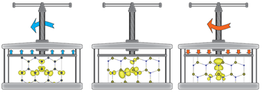
Figure 1 Tensile axial strain along c-axis in Fe-doped p-type GaN delocalizes holes, whereas compressive strain along c-axis traps the holes along strain direction.
For carrier-mediated ferromagnetism in magnetic semiconductors, such control carrier localization may even switch on and off the magnetic interaction, as well as control magnetic anisotropy. Indeed, for Mn-doped GaN, strain induced by the inverse piezoelectric effect has been shown to change anisotropic properties [3].
A simple mechanism based on electrostatics is presented to describe the control of carrier wavefunctions by the piezoelectric effect, and similar strain effects are investigated in other, non-magnetic materials.
[1] H. Raebiger et al, Phys. Rev. Mater. 2, 024402 (2018).
[2] S. Bae, H. Raebiger, Phys. Rev. B 94, 241115 (2016).
[3] D. Sztenkiel et al, Nature Commun. 7, 13232 (2016).