A research article authored by Sang Cheol Yang (KAIST EE), Junhwan Choi (KAIST CBE), Byung Chul Jang (KAIST EE), Woonggi Hong (KAIST EE), Gi Woong Shim (KAIST EE), Sang Yoon Yang (KAIST EE), Sung Gap Im (KAIST CBE), and Sung‐Yool Choi (KAIST EE; Corresponding author) was published in Advanced Electronic Materials (2019.05)
Article title: Large-Scale, Low-Power Nonvolatile Memory Based on Few-Layer MoS2 and Ultrathin Polymer Dielectrics
With the advent of artificial intelligence and the Internet of Things, demand has grown for flexible, low-power, high-density nonvolatile memory capable of handling vast amounts of information. Ultrathin-layered 2D semiconductor materials such as molybdenum disulfide (MoS2) have considerable potential for flexible electronic device applications because of their unique physical properties. However, development of flexible MoS2-based flash memory is challenging, as there is a lack of flexible dielectric materials with sufficient insulating properties for use in flash memory devices with dielectric bilayers. Here, large-scale, low-power nonvolatile memory is realized based on a chemical vapor deposition (CVD)-grown millimeter-scale few-layer MoS2 semiconductor channel and polymer dielectrics prepared via an initiated CVD (iCVD) process. Using the outstanding insulating properties and solvent-free nature of iCVD, fabricated memory devices with a tunable memory window, a high on/off ratio (≈106), low operating voltages (≈13 V), stable retention times exceeding 105 s with a possible extrapolated duration of years, and cycling endurance exceeding 1500 cycles are demonstrated. Owing to these characteristics, these devices distinctly outperform previously reported MoS2-based memory devices. Leveraging the inherent mechanical flexibility of both ultrathin polymer dielectrics and MoS2, this work is a step toward realization of large-scale, low-power, flexible MoS2-based flash memory.

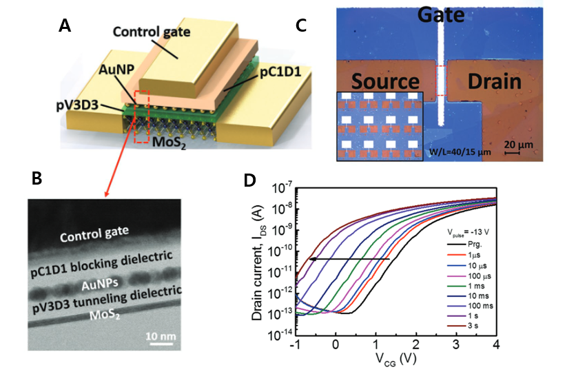
Figure 1. A Schematic illustration of fabricated MoS2-based memory device composed of pV3D3 tunneling dielectric, Au nanoparticle (NP) FG, and pC1D1 blocking dielectric layer. B Cross-sectional HRTEM image of memory device. C Optical microscopy image of fabricated 5 × 6 memory device array. D Transfer curves as functions of pulse width during erasing operation.