Abstract
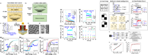
A mnemonic-opto-synaptic transistor (MOST) that has triple functions is demonstrated for an in-sensor vision system. It memorizes a photoresponsivity that corresponds to a synaptic weight as a memory cell, senses light as a photodetector, and performs weight updates as a synapse for machine vision with an artificial neural network (ANN). Herein the memory function added to a previous photodetecting device combined with a photodetector and a synapse provides a technical breakthrough for realizing in-sensor processing that is able to perform image sensing and signal processing in a sensor. A charge trap layer (CTL) was intercalated to gate dielectrics of a vertical pillar-shaped transistor for the memory function. Weight memorized in the CTL makes photoresponsivity tunable for real-time multiplication of the image with a memorized photoresponsivity matrix. Therefore, these multi-faceted features can allow in-sensor processing without external memory for the in-sensor vision system. In particular, the in-sensor vision system can enhance speed and energy efficiency compared to a conventional vision system due to the simultaneous preprocessing of massive data at sensor nodes prior to ANN nodes. Recognition of a simple pattern was demonstrated with full sets of the fabricated MOSTs. Furthermore, recognition of complex hand-written digits in the MNIST database was also demonstrated with software simulations.

Abstract
A self-powered artificial mechanoreceptor module is demonstrated with a triboelectric nanogenerator (TENG) as a pressure sensor with sustainable energy harvesting and a biristor as a neuron. By mimicking a biological mechanoreceptor, it simultaneously detects the pressure and encodes spike signals to act as an input neuron of a spiking neural network (SNN). A self-powered neuromorphic tactile system composed of artificial mechanoreceptor modules with an energy harvester can greatly reduce the power consumption compared to the conventional tactile system based on von Neumann computing, as the artificial mechanoreceptor module itself does not demand an external energy source and information is transmitted with spikes in a SNN. In addition, the system can detect low pressures near 3 kPa due to the high output range of the TENG. It therefore can be advantageously applied to robotics, prosthetics, and medical and healthcare devices, which demand low energy consumption and low-pressure detection levels. For practical applications of the neuromorphic tactile system, classification of handwritten digits is demonstrated with a software-based simulation. Furthermore, a fully hardware-based breath-monitoring system is implemented using artificial mechanoreceptor modules capable of detecting wind pressure of exhalation in the case of pulmonary respiration and bending pressure in the case of abdominal breathing.

Abstract
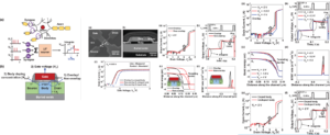
Leaky characteristic in a leaky integrate-and-fire (LIF) neuron is important to prevent a permanent effect on a single input stimulus in an artificial neuromorphic system as well as a biological nerve. In a proposed single-transistor-based LIF neuron (1T-neuron), band-to-band tunneling (BTBT) dominates the leaky characteristic. Three methods to control the leaky characteristic of a 1T-neuron are demonstrated in this work: controlling the relative location of the drain junction edge to a gate, tuning the gate voltage ( VG ), and modulating body doping concentration ( Nsub ). The 1T-neuron becomes leakier with a more overlapped drain junction with the gate, decreased VG , and increased Nsub by accelerating the BTBT.

Abstract
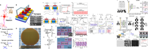
Cointegration of multistate single-transistor neurons and synapses was demonstrated for highly scalable neuromorphic hardware, using nanoscale complementary metal-oxide semiconductor (CMOS) fabrication. The neurons and synapses were integrated on the same plane with the same process because they have the same structure of a metal-oxide semiconductor field-effect transistor with different functions such as homotype. By virtue of 100% CMOS compatibility, it was also realized to cointegrate the neurons and synapses with additional CMOS circuits. Such cointegration can enhance packing density, reduce chip cost, and simplify fabrication procedures. The multistate single-transistor neuron that can control neuronal inhibition and the firing threshold voltage was achieved for an energy-efficient and reliable neural network. Spatiotemporal neuronal functionalities are demonstrated with fabricated single-transistor neurons and synapses. Image processing for letter pattern recognition and face image recognition is performed using experimental-based neuromorphic simulation.

Abstract
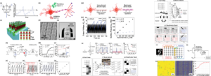
A single transistor neuron (1T-neuron) is demonstrated by using a vertically protruded nanowire from an 8 in. silicon (Si) wafer. The 1T-neuron adopts a gate-all-around structure to completely surround the Si nanowire (Si-NW) to make a floating body and allow aggressive downscaling. The Si-NW is composed of an n+ drain at the top, n+ source at the bottom, and p-type floating body at the middle, which are self-aligned vertically. Thus, it occupies a small footprint area. The gate controls an excitatory/inhibitory function. In addition, myelination of a biological neuron that changes membrane capacitance is mimicked by an inherently asymmetric source/drain structure. Two spiking frequencies at the same input current are controlled by whether the neuron is myelinated or unmyelinated. Using the vertical 1T-neuron, pattern recognition is demonstrated with both measurements and semiempirical circuit simulations. Furthermore, handwritten numbers in the MNIST database are recognized with accuracy of 93% by software-based simulations. Applicability of the vertical 1T-neuron to various neural networks is verified, including a single-layer perceptron, multilayer perceptron, and spiking neural network.

저널: Advanced Intelligent Systems
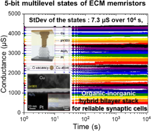
Title: Highly reliable synaptic cell array based on organic-inorganic hybrid bilayer stack toward precise offline learning
Abstract: As the use of artificial intelligence soars, development of novel neuromorphic computing is highly important because of disadvantages of the existing von Neumann architecture. In addition, extensive research on electrochemical metallization (ECM) memristors as synaptic cells have been carried out in pursuit of a linear conductance update for online learning applications. In most cases, however, a conductance distribution change during retention time while updating has not been studied as a major issue, giving less consideration for inference-only computing accelerators based on offline learning. Herein, we suggest organic-inorganic bilayer stacking for synaptic unit cells using poly(1,3,5-trivinyl-1,3,5-trimethyl cyclotrisiloxane) (pV3D3) and Al2O3 thin films, showing highly enhanced reliability for offline learning. The bilayer structure achieved better reliability and control of the analog resistive switching and synaptic functions, respectively, through the guided formation of conductive filaments via tip enhanced electric fields. In addition, 5-bit multilevel states achieved long-term stability (> 104 s) following an in-depth study on conductance-level stability. Finally, a device to-system-level simulation was performed by building a CNN based on the hybrid devices. This highlighted the significance of multilevel states in fully connected layers. We believe that our study provides a practical approach to using ECM-based memristors for inference-only neural network accelerators.

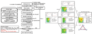
제목: Bayesian Optimization of MOSFET Devices Using Effective Stopping Condition
논문지, 연도: IEEE Access, 2021
저자: Bokyeom Kim and Mincheol Shin
초록: Current nanometer-scale metal-oxide-semiconductor field-effect transistor (MOSFET) devices exhibit short-channel, quantum, and self-heating effects, making modeling and analysis very complex. A few recent works have employed machine-learning (ML) techniques and neural networks (NN) to model the complex relationships and optimize devices, but a problem with the NN-based device optimization is that it is data-intensive. Bayesian optimization (BO) can realize ML-based data-efficient optimization of the MOSFET device, as it finds the global optimum while requiring few training data. BO stops theoretically when every candidate is explored, so previous works used a fixed number of iterations for the stopping condition. Such an empirical stopping condition is detrimental to the efficiency and reliability of BO, because the global optimum can be found at an earlier stage or even after stopping. Recently, maximum expected improvement (EI max ) with a tiny constant has been proposed as a stopping condition for BO. However, there have not been sufficient works for improving efficiency of BO. By advancing the EI max scheme, we have systemically investigated the effective stopping condition (ESC) for BO of MOSFET devices to boost the efficiency and reliability of optimization. We found that EI max less than a 1% of unit value was an efficient and reliable ESC for optimization, which resulted in up-to-87.6% and up-to-47% reductions of required training data compared with the fixed iteration method and the tiny constant method, respectively. Our study provides a novel method to boost efficiency and reliability of BOs for the optimization of MOSFET design in the semiconductor industry.

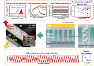
Title: Reliable multilevel memristive neuromorphic devices based on amorphous matrix via quasi-1D filament confinement and buffer layer
Conference/Journal, Year: Science Advances, 2022
Author: Sang Hyun Choi, See-On Park, Seokho Seo, and Shinhyun Choi
Abstract: Conductive-bridging random access memory (CBRAM) has garnered attention as a building block of non–von Neumann architectures because of scalability and parallel processing on the crossbar array. To integrate CBRAM into the back-end-of-line (BEOL) process, amorphous switching materials have been investigated for practical usage. However, both the inherent randomness of filaments and disorders of amorphous material lead to poor reliability. In this study, a highly reliable nanoporous–defective bottom layer (NP–DBL) structure based on amorphous TiO2 is demonstrated (Ag/a-TiO2/a-TiOx/p-Si). The stoichiometries of DBL and the pore size can be manipulated to achieve the analog conductance updates and multilevel conductance by 300 states with 1.3% variation, and 10 levels, respectively. Compared with nonporous TiO2 CBRAM, endurance, retention, and uniformity can be im-proved by 106 pulses, 28 days at 85°C, and 6.7 times, respectively. These results suggest even amorphous-based systems, elaborately tuned structural variables, can help design more reliable CBRAMs.

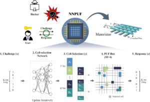
Title: Neural Network Physically Unclonable Function: A Trainable Physically Unclonable Function System with Unassailability against Deep Learning Attacks Using Memristor Array
Conference/Journal, Year: Advanced Intelligent Systems, 2021
Author: Junkyu Park, Yoonji Lee, Hakcheon Jeong, and Shinhyun Choi
Abstract:
The dissemination of edge devices drives new requirements for security primitives for privacy protection and chip authentication. Memristors are promising entropy sources for realizing hardware-based security primitives due to their intrinsic randomness and stochastic properties. With the adoption of memristors among several technologies that meet essential requirements, the neural network physically unclonable function (NNPUF) is proposed, a novel PUF design that takes advantage of deep learning algorithms. The proposed design integrated with the memristor array can be constructed easily because the system does not depend on write operation accuracy. To contemplate a nondifferentiable module during training, an original concept of loss called PUF loss is devised. Iterations of weight update with the loss function bring about optimal NNPUF performance. It is shown that the design achieves a near-ideal 50% average value for security metrics, including uniformity, diffuseness, and uniqueness. This means that the NNPUF satisfies practical quality standards for security primitives by training with PUF loss. It is also demonstrated that the NNPUF response has an unassailable resistance against deep learning-based modeling attacks, which is verified by the near-50% prediction model accuracy.

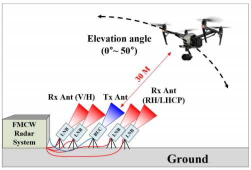
우리 학부 박성욱 교수와 박사과정 강현성 학생이 CNN(Convolutional neural network, 인공신경망의 한 종류)으로 MDS (micro-Doppler signature, 드론을 레이더로 감지하기 위한 신호 중 하나)를 분류하여 실제 드론의 이륙 각도를 감지하는 기술을 개발하였습니다.
드론에 대한 기술이 빠르게 발전함에 따라, 농업, 화물 운송, 영상 수집 등 그에 따른 많은 장점도 있으나 불법적으로 드론을 악용하는 사례나 드론으로 인한 사고로 인한 문제점이 늘어가고 있습니다. 이로 인한 문제점을 지속적으로 관리하고 방지하기 위해, 공중에 떠 있는 드론을 정확하게 인식하고 그 위치를 파악하는 연구가 활발하게 진행되고 있습니다. 하지만 현재의 기술은 대부분 수 킬로미터 한정의 레이더 감지가 가능하며, 공간적인 한계를 극복하기 위해 넓게 분포된 저렴한 레이더 네트워크 방식이 쓰였으나 이로 인해 하나의 레이더가 감지해야 할 이륙 각도의 범위가 넓어지게 되었습니다. 하지만 대부분의 레이더는 팬 빔 (fan beam)을 회전시키면서 스캔하므로 정확한 이륙 각도의 감지가 어렵습니다.
본 연구팀은 이러한 레이더의 한계를 극복하면서도 값싼 레이더 네트워크 방식을 유지하기 위해, 드론에서부터 얻을 수 있는 MDS 라는 신호와 CNN (합성곱신경망)을 이용해 드론의 이륙 각도를 비교적 정확하게 분류하는 방식을 개발하였습니다. 또한, 이러한 인공 신경망의 분류 효율을 높이기 위해 다양한 극성 (polarization) 변수도 이용하였습니다. 결과적으로, 극성 변수의 종류를 늘려감에 따라 84.75%의 효율에서 97.9%의 효율까지 정확해진 결과를 발표하였습니다.
본 성과는 “IEEE Geoscience and remote sensing letters” 에 2020년 11월 2일자에 온라인 출판되었습니다. 자세한 내용은 아래 링크에서 확인하실 수 있습니다.
논문: https://ieeexplore.ieee.org/document/9246564
그림: 레이더 네트워크를 이용한 드론 이륙각도 인식에 대한 개요
