Home

School of Electrical Engineering We thrive
to be the world’s
top IT powerhouse.
We thrive to be the world’s top IT powerhouse.

Our mission is to lead innovations
in information technology, create lasting impact,
and educate next-generation leaders of the world.

  • 1
  • 6
Learn More
School of Electrical Engineering We thrive
to be the world’s
top IT powerhouse.
We thrive to be the world’s top IT powerhouse.

Our mission is to lead innovations
in information technology, create lasting impact,
and educate next-generation leaders of the world.

  • 2
  • 6
Learn More
School of Electrical Engineering We thrive
to be the world’s
top IT powerhouse.
We thrive to be the world’s top IT powerhouse.

Our mission is to lead innovations
in information technology, create lasting impact,
and educate next-generation leaders of the world.

  • 3
  • 6
Learn More
School of Electrical Engineering We thrive
to be the world’s
top IT powerhouse.
We thrive to be the world’s top IT powerhouse.

Our mission is to lead innovations
in information technology, create lasting impact,
and educate next-generation leaders of the world.

  • 4
  • 6
Learn More
School of Electrical Engineering We thrive
to be the world’s
top IT powerhouse.
We thrive to be the world’s top IT powerhouse.

Our mission is to lead innovations
in information technology, create lasting impact,
and educate next-generation leaders of the world.

  • 5
  • 6
Learn More
AI in EE AI and machine learning
are a key thrust
in EE research
AI and machine learning are a key thrust in EE research

AI/machine learning  efforts are already   a big part of   ongoing
research in all 6 divisions - Computer, Communication, Signal,
Wave, Circuit and Device - of KAIST EE 

  • 6
  • 6
Learn More
Previous slide
Next slide

Highlights

Inline image 2024 05 07 16.27.35.812

B.S. Candidate Do A Kwon (Prof. Jae-Woong Jeong) wins Outstanding Poster Award at the 2024 Spring Conference of The Korean Sensors Society & Sensor Expo Korea-Forum
 

Inline image 2024 05 07 16.24.45.825

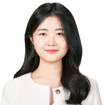
<B.S. Candidate Do A Kwon>
 

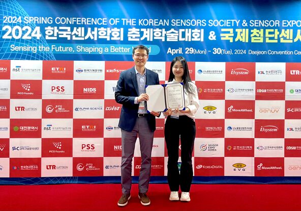
B.S. student Do A Kwon (Advised by Jae-Woong Jeong) won the Outstanding Poster Award at the 2024 Spring Conference of The Korean Sensors Society & Sensor Expo Korea-Forum. 


The Conference of the Korean Sensors Society is held biannually in spring and fall. This spring, it was held at the Daejeon Convention Center (DCC) from April 29 to 30th.

Do A Kwon, an undergraduate student, published a paper titled “Body-temperature softening electronic ink for additive manufacturing of transformative bioelectronics via direct writing” and was selected as the winner in recognition of her excellence.


The paper introduces body-temperature softening electronic ink that can be patterned in high resolution.

It is expected to open unprecedented possibilities in personalized medical devices, wearable electronics, printed circuit boards, soft robots, and more, pushing the existing limitations in electronic devices with fixed form factors.


0 Conference: 2024 Spring Conference of The Korean Sensors Society 

0 Date: April 29-30, 2024

0 Award: Outstanding Poster Award

0 Authors: Do A Kwon, Simok Lee, Jae-Woong Jeong (Advisory Professor)

0 Paper Title: Body-temperature softening electronic ink for additive manufacturing of transformative bioelectronics via direct writing 
 

Inline image 2024 05 07 16.27.35.812

<(from left) Professor Jae-Woong Jeong, Do A Kwon>
 

66332a8fd5b25

EE Professor Joung-Ho Kim Establishes NAVER-Intel-KAIST AI Joint Research Center(NIK AI Research Center) for the Development of Next-Generation AI Semiconductor Eco-System

Inline image 2024 04 30 13.39.42.721 1

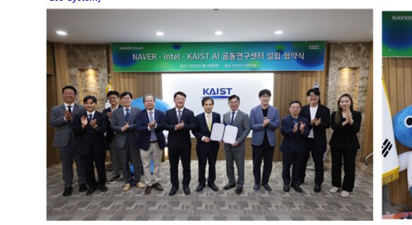
<MoU Singing Ceremony of Joint Research Center>
 
As generative AI, sparked by ChatGPT, sweeps the globe, Professor Joung-Ho Kim(KAIST), is joining forces with Naver and Intel to consolidate their capabilities and strengths in the new “NAVER·Intel·KAIST AI Joint Research Center (NIK AI Research Center)” to establish an ecosystem for new AI semiconductors.
 
Industry professionals view the strategic partnership between these three institutions as a proactive challenge to establish a new AI semiconductor ecosystem and secure market and technological leadership. They aim to integrate their individual hardware and software technologies and infrastructures in AI, including the development of open-source software necessary for the operation of AI semiconductors, AI servers, and data centers.
In particular, it is noteworthy that Intel, a global semiconductor company known for advanced CPU design and foundry capabilities, is establishing and supporting a joint research center at a domestic university—KAIST—for the first time. This initiative aims to develop open-source software and other necessary tools to optimally operate Intel’s AI semiconductor, “GAUDI”, marking a significant step beyond traditional central processing units (CPUs).
KAIST announced on the 30th that it has signed a Memorandum of Understanding (MOU) to establish and operate the “NAVER·Intel·KAIST AI Joint Research Center (NIK AI Research Center)” at its main campus in Daejeon. This collaboration with Naver Cloud, led by CEO Yu-won Kim, focuses on developing advanced open-source software aimed at enhancing the performance and optimizing the operation of AI semiconductors, AI servers, clouds, and data centers.
A KAIST representative emphasized the significance of Intel’s decision, stating, “It is of great strategic importance that Intel has chosen Naver and KAIST as partners for the development of open-source software in the fields of AI and semiconductors.“
 
The representative further detailed, “The combination of Naver Cloud’s excellence in computing, databases, and various AI services based on the NAVER Cloud Platform, Intel’s next-generation AI chip technology, and KAIST’s world-class expertise and software research capabilities, is expected to successfully create a distinctively creative and innovative ecosystem in the AI semiconductor sector.”
At the MOU signing ceremony, key KAIST officials including President Kwang-Hyung Lee, Provost and Executive Vice President Gyun-Min Lee, Senior Vice President for Research Sang-yup Lee, and Professor Joung-Ho Kim from the Department of Electrical Engineering were present. From Naver Cloud, key executives such as CEO Yu-won Kim, Head of AI Innovation Jung-Woo Ha, and Executive Officer Dong-soo Lee, responsible for Hyperscale AI, also attended.
 
Following the MOU signing, KAIST and Naver Cloud plan to establish the “NAVER·Intel·KAIST AI Joint Research Center (NIK AI Research Center)” at KAIST within the first half of the year. They are scheduled to commence full-scale research activities starting in July.
At KAIST, Professor Joung-Ho Kim of the Department of Electrical Engineering, recognized globally as a leading scholar in AI semiconductor design and AI application design (AI-X), will co-lead the NIK AI Research Center. From Naver Cloud, Executive Officer Dong-soo Lee, an expert in AI semiconductor design and AI software, will serve as the other co-director of the center. Additionally, Professor Min-hyuk Sung from the KAIST Department of Computer Science and Naver Cloud’s Leader Se-jung Kwon will each serve as deputy directors, collaboratively steering the center’s research initiatives.
 
The operation period of the joint research center is initially set for three years, with the possibility of extension based on research outcomes and the needs of the participating institutions. As a key research center, about 20 faculty members specializing in artificial intelligence and software from KAIST, along with approximately 100 master’s and doctoral students, will participate as researchers, ensuring the center is equipped with substantial expertise and innovation capacity.
During the initial two years, the joint research center will focus on establishing a platform ecosystem specifically for the AI training and inference chip, “GAUDI”, developed by Intel’s Habana Labs. To achieve this, approximately 20 to 30 collaborative industry-academic research projects will be conducted.
 
Research at the joint research center primarily focuses on the development of open-source software in fields such as natural language processing, computer vision, and machine learning. Of the center’s research efforts, 50% is devoted to autonomous subject research, while 30% and 20% of the efforts are allocated to studies on the miniaturization and optimization of AI semiconductors, respectively.
To facilitate this research, Naver and Intel will provide the “GAUDI 2”—based on the Naver Cloud Platform—to the KAIST Joint Research Center. In turn, the KAIST research team will utilize “GAUDI 2” for their studies and annually publish their findings and papers related to this work.
 
Additionally, beyond their existing capabilities in artificial intelligence and cloud technologies, Naver and Intel will share various infrastructure facilities and equipment necessary for joint research. They also plan to engage in numerous collaborative activities, including supporting the joint research center with the necessary space and administrative staff and facilitating the exchange of research personnel between the institutions. This comprehensive support is designed to enhance the effectiveness and impact of their cooperative efforts.
Professor Joung-Ho Kim of highlighted the significant benefits of the joint research center, stating, “KAIST can acquire technical know-how in AI development, semiconductor design, and operational software development through the use of the GAUDI series. Particularly, the establishment of this joint research center is highly meaningful as it allows us to gain experience in operating large-scale AI data centers and to secure the AI computing infrastructure needed for future research and development.”
Director Dong-soo Lee from Naver Cloud expressed his aspirations for the collaboration: “Naver Cloud looks forward to leading various research initiatives with KAIST and expanding the AI ecosystem centered around HyperCLOVA X. Through the joint research center, we hope to invigorate AI research in the country and enhance the diversity of the AI chip ecosystem.” 
 
[ Terminologies ]
* Generative AI
: Artificial intelligence technology that uses deep learning models to learn from large datasets. It can actively generate outputs such as text, images, and videos based on user requests.
** GAUDI
: A general-purpose AI accelerator for data centers, developed by Habana Labs, an Israeli AI chip company acquired by Intel in 2019.
*** High Bandwidth Memory (HBM)
: A high-performance DRAM technology where multiple DRAM chips are interconnected using Through Silicon Vias (TSVs) to significantly enhance data processing speeds. It is primarily used in conjunction with GPUs to accelerate AI training and generation speeds. Characteristically, HBM is designed to maximize memory bandwidth, making it especially suitable for high-speed parallel processing. It is a critical semiconductor in AI computers installed in mega-scale generative AI data centers. The technology has evolved through several generations: HBM, HBM2, HBM2E, HBM3, and the current HBM3E. Companies like Samsung Electronics and SK Hynix are currently developing HBM4, which is used in GPU modules by NVIDIA, Intel, and AMD.


2 2

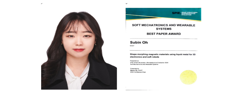
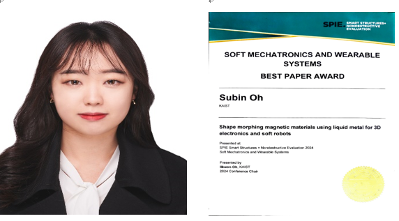
EE Ph.D. candidate Subin Oh (Prof. Jae-Woong Jung) wins Best Paper Award at SPIE Smart Structures + NDE 2024                 
  Inline image 2024 04 25 13.51.35.243

<(From left) Ph.D. candidate Subin Oh, Award Certificate>


Ph.D. student Subin Oh (Advised by Jae-Woong Jeong) won the Best Paper Award at SPIE Smart Structures + NDE 2024.

The SPIE Smart Structures + NDE brings together engineers and researchers as they share important advances that help move multifunctional materials, sensor systems, and structural health monitoring technologies into the future. 

This conference was held from March 25 to 28 in Los Angeles, USA with over 450 papers presented. Ph.D. student Subin Oh presented the paper titled “Shape morphing magnetic materials using liquid metal for 3D electronics and soft robots”.
 

GLhMuWRa0AAY7EI

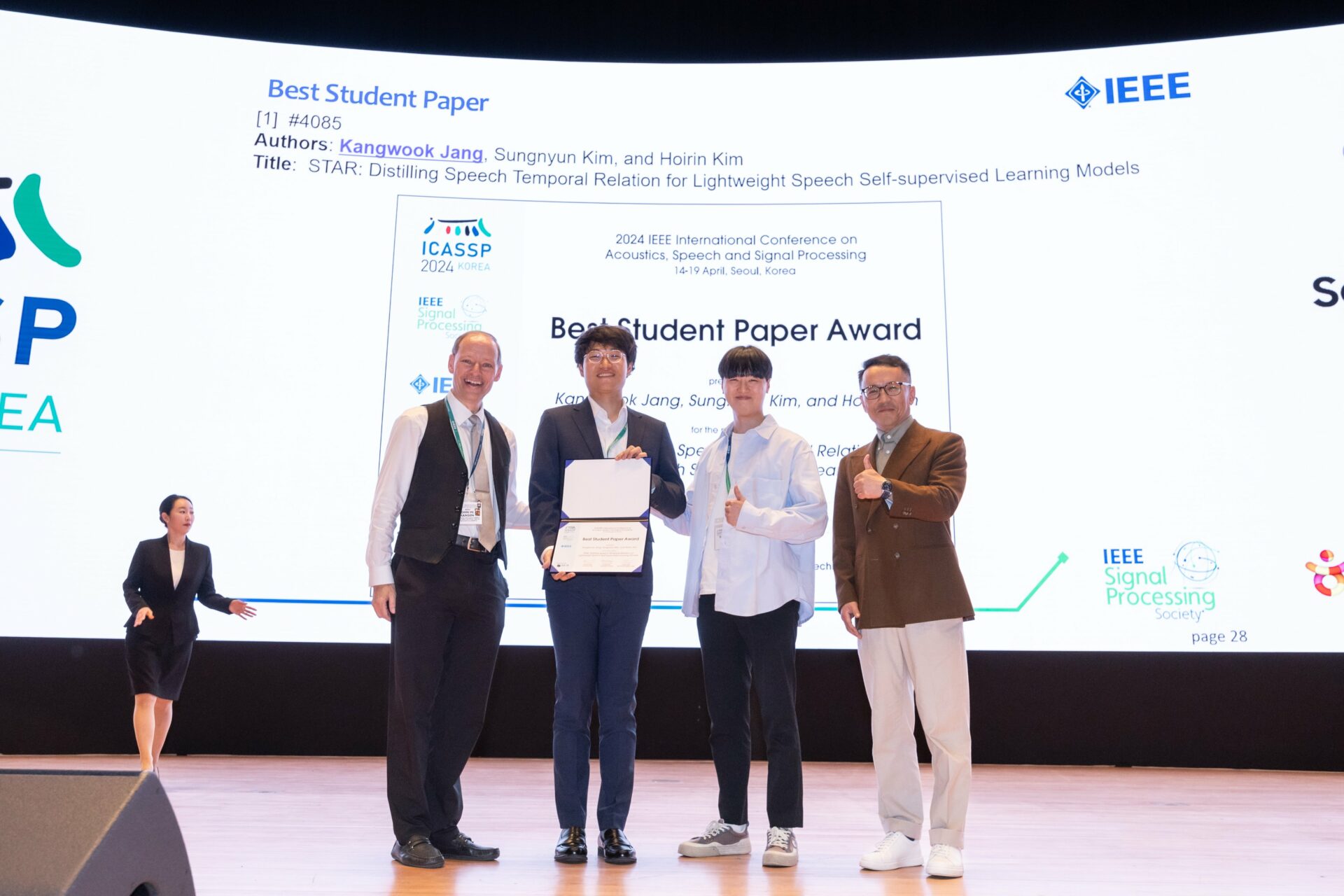
Professor Hoirin Kim’s research team wins ‘Best Student Paper Award’ at the International Conference on Acoustics, Speech, and Signal Processing (ICASSP)

<(From left) Certificate of Award, Award ceremony, PhD candidate Kangwook Jang (first author), PhD candidate Sungnyun Kim>
 
The research team of Prof. Hoirin Kim from our school has won the Best Student Paper Award at the IEEE International Conference on Acoustics, Speech, and Signal Processing, one of the top-tier international signal, speech, and acoustics conferences. This honor is only given to the top five papers from academic institutions out of 5,576 submitted papers.
 
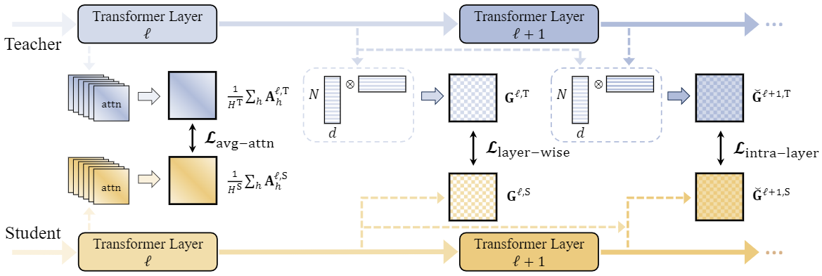
The research team, consisting of Kangwook Jang (first author) from the School of Electrical and Electronic Engineering, Sungnyun Kim from the Graduate School of AI, and Professor Hoirin Kim, won the Best Student Paper Award by proposing a new distillation loss function for compressing of speech self-supervised learning (speech SSL) models using the speech temporal relation as a new distillation loss function.
 
Although speech self-supervised learning models perform well on various speech tasks such as speech recognition and speaker verification, it is still not sufficient for practical scenarios, such as on-device application, due to the very large number of parameters. Therefore, there has been a lot of researches on compression to reduce the number of parameters of these models through knowledge distillation (KD). However, most of the current techniques directly match the teacher’s speech representation to the student, which is over-constraint for students with weak model representation.
 
Untitled
<Schematic diagram of the speech temporal relation loss function proposed by Prof. Hoirin Kim’s research team>
 
Prof. Hoirin Kim’s research team has explored various objectives to express the temporal relation between speech frames and proposed a loss function suitable for speech self-supervised learning models. The compressed student model is validated on a total of 10 speech-related tasks, and it performs the best among the models that compressed the parameters by about 30%.
 
This research was supported by the National Research Foundation of Korea grant funded by Korea government.


2 1

Professor Kyeongha Kwon’s Research Team Develops a Bioelectronic System for Monitoring Bladder Function After Surgery Using Electronic Sensors


images 000076 photo1.jpg 6

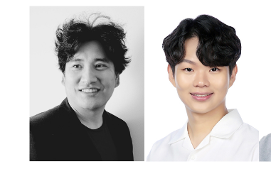
<(from left) Professor Kyeongha Kwon, Doyun Park (Master’s student), Dr. Jihye Kim from Nothwestern University>
 
 
A bioelectronic system has been developed to safely monitor bladder function without the need for catheter insertion in patients who have undergone cystectomy, making it a topic of interest.

 *A catheter is a thin tube made of rubber or metal that is inserted into the bladder.

The research team led by Professor Kyeongha Kwon from the School of Electrical Engineering at KAIST announced on the 16th that they have developed digital healthcare technology that accurately measures the size and pressure changes of the bladder through joint research with Dr. Jihye Kim from Northwestern University in the United States.

Partial cystectomy* requires a long recovery period, during which the urinary tract’s ability to expel urine externally is intermittently assessed through urodynamic studies** (UDS). However, UDS is not patient-friendly, results can vary among users, and it is limited in its ability to collect continuous data. Furthermore, it can lead to the risk of catheter-associated urinary tract infections and, in high-risk patients, can progress to ascending pyelonephritis. As an appropriate alternative to UDS, there is a need for technology that can continuously and in real-time monitor the condition of the bladder without the insertion of a catheter.
 
  *Partial cystectomy: A surgery that involves cutting out the tumor-bearing part of the bladder and stitching the rest of the bladder back together.

  **Urodynamic studies: Diagnostic tests to assess the overall function of the bladder and urethra to plan treatment.

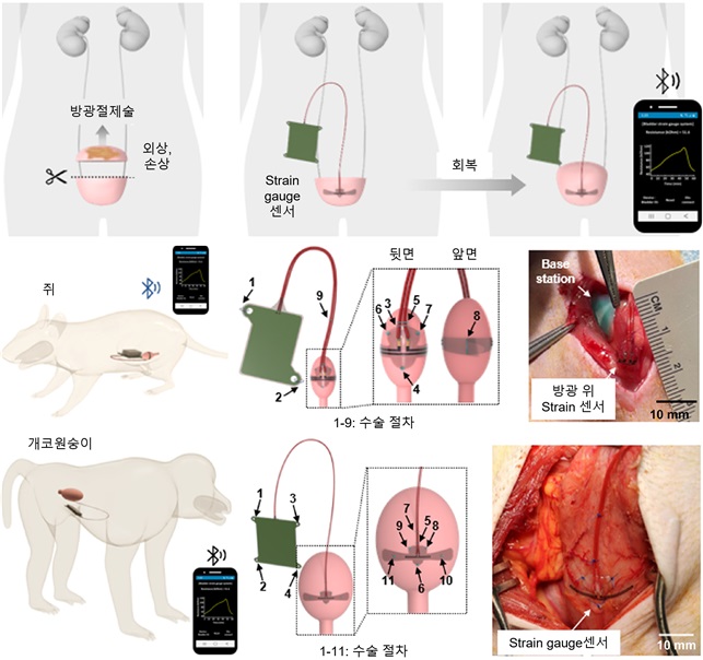
In response, the research team developed an implantable bladder platform that can wirelessly remotely measure mechanical deformation changes related to bladder filling and emptying. This system uses biodegradable strain sensors to measure the size and pressure changes of the bladder in real-time, and the sensors naturally dissolve and disappear within the body after the recovery period. This eliminates the need for additional surgery to remove the monitoring equipment, reduces the risk of complications, and improves patient comfort and recovery time.
 
 
images 000076 image1 1.jpg 6 1
<Figure 1. Wireless implantable platform for bladder function monitoring (top), mouse model experimental setup (middle), Baboon experimental setup (bottom)>
 
The team proved through mouse models that this platform could reproduce real-time changes for up to 30 days after implantation. Additionally, through experiments on marmosets, the technology demonstrated consistency in pressure measurements for up to eight weeks compared to traditional UDS. These results suggest that the system can be used as an appropriate alternative to UDS for long-term post-surgical bladder recovery monitoring.

Professor Kyeongha Kwon said, “Through extensive experiments using non-human primates (marmosets), we have demonstrated the efficacy of a device that provides accurate and reliable data on bladder function,” and added, “This can be used to shorten patients’ recovery time and improve overall surgical outcomes.”

The results of this study were published in the ‘Proceedings of the National Academy of Sciences (PNAS)’ on April 2nd. (Article title: A wireless, implantable bioelectronic system for monitoring urinary bladder function following surgical recovery, link: https://www.pnas.org/doi/abs/10.1073/pnas.2400868121?af=R)

This research was conducted with the support of the Basic Research Program, the Regional Innovation Lead Research Center Project, and BK21 funded by the Ministry of Science and ICT and the National Research Foundation of Korea.
 

2

Professor Shinhyun Choi’s Research Team Develops Novel Semiconductor Device for Next-Generation Neuromorphic Computing/Memory (Published in Nature)
 

Inline image 2024 04 03 15.57.51.490

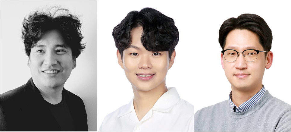
<(left) Professor Shinhyun Choi, See-On Park integrated ph.d. candidate, Seokman Hong ph.d. candidate>
 

On the 4th, Professor Shinhyun Choi’s research team announced that they have developed an ultra-low power next-generation phase-change memory device that can replace DRAM (Dynamic Random-Access Memory) and NAND flash memory.

☞ Phase Change Memory: A memory device that stores or processes information by changing the resistance state through the use of heat to alter the material between amorphous and crystalline states.


Existing phase change memory devices are manufactured through expensive ultra-fine semiconductor lithography processes, requiring high power consumption. Previous research has focused on reducing the physical size of the device using ultra-fine semiconductor lithography processes to increase the heating effect for memory operation and lower power consumption.


However, this approach achieved only minor improvements in power efficiency and faced practical limitations due to increased process costs and complexity. Professor Choi’s team developed an ultra-low power phase change memory device that electrically forms extremely small nanometer-scale phase change filaments without the need for expensive lithography processes.

This not only significantly reduces process costs but also enables ultra-low power operation, offering a revolutionary advantage.


To address the power consumption issue of phase change memory, Professor Choi’s research team successfully developed an ultra-low power phase change memory device that consumes over 15 times less power than existing devices made through expensive ultra-fine lithography processes. This was achieved by electrically forming the phase change material in an extremely small manner.

EE Ph.D. candidates Park See-On and Hong Seokman participated as the first authors in this study. The research was published in the April issue of the renowned international academic journal `Nature’ on April 4th. (Paper title: Phase-Change Memory via a Phase-Changeable Self-Confined Nano-Filament)
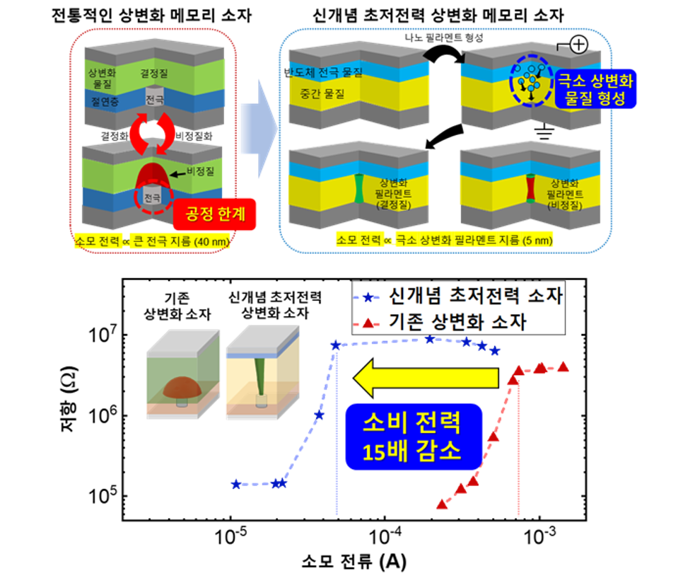
 

image 1

< Figure 1: Diagram of the ultra-low power phase change memory device developed in this study, and a comparison of the power consumption reduction of the ultra-low power phase change memory device to existing phase change memory devices>


This research was supported by the Korea Research Foundation’s Next-Generation Intelligent Semiconductor Technology Development Project, the PIM Artificial Intelligence Semiconductor Core Technology Development (Device) Project, the Excellent Young Researcher Program, and the Nano Medical Device Development Project of the Nano Institute of Technology.
 

Professor Yang-Kyu Choi’s Research Team Solved Computing Challenges with Neuromorphic Neural Networks
 

images 000075 photo1.jpg 13

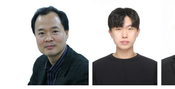
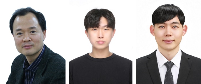
<(from left) Professor Yang-Kyu Choi, ph.d. candidate Seong-Yun Yun, Professor Joon-kyu Han from Sogang University (KAIST alumnus)>
 
 
Professor Yang-Kyu Choi’s research team has built a miniature oscillatory neural network using only silicon materials and processes currently used in the semiconductor industry, implementing an edge detection feature and solving the graph coloring problem*.


*Graph coloring problem: A term used in graph theory, requiring different colors to be assigned to each vertex of a graph. This is similar to assigning frequencies to broadcasting stations to prevent overlap and the creation of areas with poor reception, and is widely applied in various fields.


The research team announced on the 3rd that they have developed a neuromorphic oscillatory neural network that mimics the interactions of biological neurons using silicon varistor components.


With the arrival of the big data era, artificial intelligence technology has made significant progress. One of the neuromorphic computing methods, the oscillatory neural network (oscillatory neural network), is an artificial neural network that mimics the interaction of neurons. The oscillatory neural network uses the connection operations of oscillators, which are the basic units, and performs calculations using oscillations rather than the magnitude of signals, thus offering advantages in terms of power consumption.
 
 
images 000075 image1.jpg 12
 
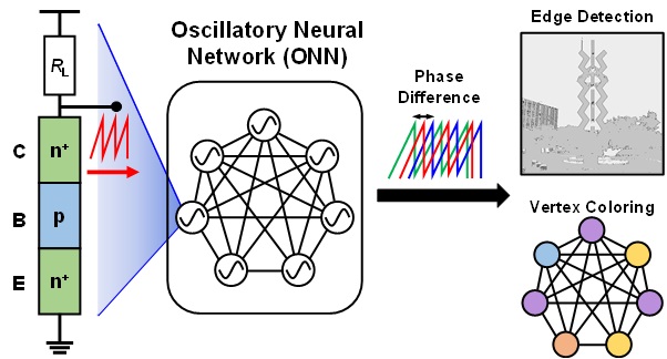
< Figure 1. The oscillatory neural network using varistors and its applications >


The research team developed the oscillatory neural network using silicon-based oscillators. By connecting two or more silicon oscillators using capacitors, the oscillation signals interact with each other and synchronize over time. The research team implemented edge detection, a feature used in image processing, with the oscillatory neural network and solved one of the challenges, the vertex coloring problem.


Furthermore, this research has the advantage of being immediately applicable to mass production from a manufacturing perspective, as it built the oscillatory neural network using only silicon materials and processes currently used in the semiconductor industry, instead of complex circuits or materials and structures with low compatibility with existing semiconductor processes.


The research, led by Seong-Yun Yun, a doctoral student, and Professor Joon-Kyu Han from Sogang University, stated, “The developed oscillatory neural network can be used as neuromorphic computing hardware capable of calculating complex computing challenges, and is expected to be useful in resource allocation, new drug development, semiconductor circuit design, and scheduling,” highlighting the significance of the research.


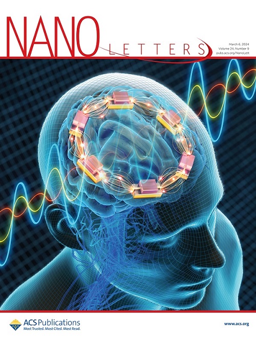
The study, co-authored by Seong-Yun Yun and Professor Joon-Kyu Han, was published in ‘Nano Letters’, in its 24th volume, issue 9, on March 2024, and was selected as a supplementary cover article.
 
images 000075 image2.jpg 9
Photo Caption: < Figure 2. The image selected as a supplementary cover article for Nano Letters >

(Paper title: A Nanoscale Bistable Resistor for an Oscillatory Neural Network) (https://pubs.acs.org/doi/full/10.1021/acs.nanolett.3c04539). 

This research was conducted with the support of the Korea Research Foundation’s Next-Generation Intelligent Semiconductor Technology Development Project and the National Semiconductor Research Laboratory Support Core Technology Development Project.
2 1

Professor Kyeongha Kwon Appointed as Korea Representative of the IEEE ISSCC TPC
 

Inline image 2024 03 25 11.23.06.169

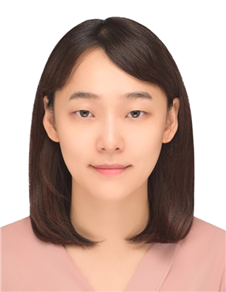
<Professor Kyeongha Kwon>
 
Prof. Kyeongha Kwon has been appointed as the Korea Representative for the Technical Program Committee (TPC) of the International Solid-State Circuits Conference (ISSCC), organized by the Institute of Electrical and Electronics Engineers (IEEE).
 
Held annually in February in San Francisco, USA, ISSCC is internationally recognized as the leading authority in the semiconductor field, often referred to as the “Semiconductor Olympics.” Since its inception in 1954, the conference has been a gathering point for over 4,000 semiconductor engineers from around the world, who come together to exchange the latest research findings and discuss the future of the semiconductor industry.
 
The selection of papers for presentation and the organization of lectures and discussion programs at the conference are managed by 12 TPCs, composed of researchers from academia and industry across various countries, all recognized for their academic achievements.
 
Currently, there are a total of 23 TPC members active in Korea, including 8 from Samsung Electronics, 1 from SK Hynix, 4 from KAIST, and one each from DGIST, GIST, UNIST, Korea University, Sogang University, Seoul National University, Yonsei University, Ewha Womans University, and POSTECH, with one member representing Sapeon.
 
Prof. Kwon began her activities as a TPC member in 2023 and has been appointed as the country representative this year.
Prof. Kwon will preside over meetings of the TPC members in Korea, press conferences, etc., and will facilitate interactions with country representatives from other nations, contributing to the advancement of semiconductor technology.


NOTICE

MORE

SCHEDULE

SEMINAR