to be the world’s
top IT powerhouse.We thrive to be the world’s top IT powerhouse.
Our mission is to lead innovations
in information technology, create lasting impact,
and educate next-generation leaders of the world.
- 1
- 6
to be the world’s
top IT powerhouse.We thrive to be the world’s top IT powerhouse.
Our mission is to lead innovations
in information technology, create lasting impact,
and educate next-generation leaders of the world.
- 2
- 6
to be the world’s
top IT powerhouse.We thrive to be the world’s top IT powerhouse.
Our mission is to lead innovations
in information technology, create lasting impact,
and educate next-generation leaders of the world.
- 3
- 6
to be the world’s
top IT powerhouse.We thrive to be the world’s top IT powerhouse.
Our mission is to lead innovations
in information technology, create lasting impact,
and educate next-generation leaders of the world.
- 4
- 6
to be the world’s
top IT powerhouse.We thrive to be the world’s top IT powerhouse.
Our mission is to lead innovations
in information technology, create lasting impact,
and educate next-generation leaders of the world.
- 5
- 6
are a key thrust
in EE researchAI and machine learning are a key thrust in EE research
AI/machine learning efforts are already a big part of ongoing
research in all 6 divisions - Computer, Communication, Signal,
Wave, Circuit and Device - of KAIST EE
- 6
- 6
develops a simulation
framework called vTrain
Achieves Human-Level Tactile Sensing with
Breakthrough Pressure Sensor
Seungwon Shin’s Team
Validates Cyber Risks
of LLMs
Wearable Carbon Dioxide Sensor
Joint Team Develops
Neuromorphic Semiconductor Chip
Develops High-Efficiency
Avalanche Quantum Dots
Develop AI That
Imagines and Understands
Microelectrodes Array
Hafnia-Based Ferroelectric Memory Technology
Highlights

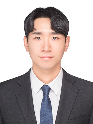
Dr. Hyeongtaek Lee, a graduate of the Intelligent Communication Systems Lab. (ICL) in the School of Electrical Engineering (Advisor: Prof. Junil Choi), has been appointed as an Assistant Professor in the Dept. of Electronic and Electrical Engineering at Ewha Womans University, effective March 1, 2025.
Dr. Hyeongtaek Lee received Ph.D. degree from the School of Electrical Engineering at KAIST in August 2023, and has since served as a postdoctoral research at Institute of Information Electronics, KAIST.
His primary research focuses on the development of 6G wireless communication systems. He has published papers at top-tier journals such as IEEE TWC and IEEE TCOM, and the excellence and practicality of his research have been recognized through a number of best paper awards and international patent registrations.
At Ewha Womans University, he will continue to develop practical algorithms for future wireless communication systems.
<Dr. Jihoon Sung >
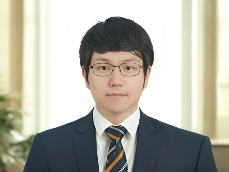
Dr. Jihoon Sung, a graduate of the Quantum Information and Communications Lab. (QUIC) in the Department of Electrical Engineering at KAIST (Advisor: Prof. June-Koo Rhee), has been appointed as a tenure-track faculty member in the School of Computer and Artificial Intelligence, College of Engineering, Jeonbuk National University, effective March 1, 2025.
After earning his Ph.D. from KAIST in August 2016, Dr. Sung worked at Samsung Electronics’ Mobile Experience Business (MX) Division for four years, where he developed and commercialized various network technologies, including wireless network optimization and security solutions utilizing AI/ML technologies. Since September 2020, he has been conducting research at ETRI, focusing on network intelligence, automation, and optimization. His work has also contributed to securing standard-essential patents related to the standard technologies of the 3GPP, a key standardization body in the field of mobile communication technologies.
His primary research interests lie in network intelligence and optimization, and he has published multiple papers in renowned international journals, including IEEE TMM.
Moving forward, he aims to advance research in network intelligence and high-level network technologies by integrating AI/ML technologies into the networking field.
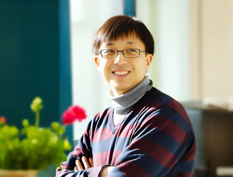 <Prof. John Kim>
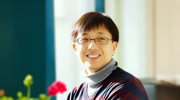
Prof. John Kim has been elevated to IEEE Fellow, class of 2025, “for contributions to the design and analysis of high-performance interconnection network architectures.” Prof. Kim’s research area is in computer architecture and interconnection networks. As systems scale-up and scale-out with more components, data movement is becoming a bigger bottleneck in modern digital systems. Prof. Kim’s research addresses the communication bottleneck in multi-core and large-scale systems and his research lab is also currently exploring communication bottlenecks in deep-learning systems.
Prof. Kim’s research has led him to become the first researcher from Asia to be inducted into the hall-of-fame for all three main computer architecture conferences — ISCA, MICRO, and HPCA. He was also the first researcher from an Asia institution to serve as the program chair for a top-tier computer architecture conference (HPCA’24). Prof. Kim plans on pursuing research on efficient data movement across memory-centric architectures and exploiting domain-specific networks.
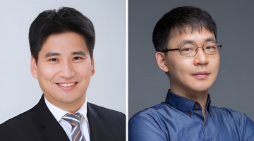
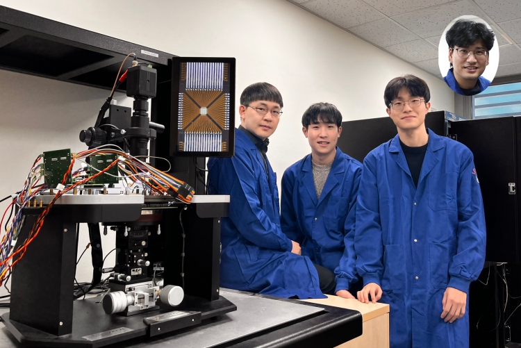
Existing computer systems have separate data processing and storage devices, making them inefficient for processing complex data like AI. EE research team has developed a memristor-based integrated system similar to the way our brain processes information. It is now ready for application in various devices including smart security cameras, allowing them to recognize suspicious activity immediately without having to rely on remote cloud servers, and medical devices with which it can help analyze health data in real time.
The joint research team of Professor Shinhyun Choi and Professor Young-Gyu Yoon of the School of Electrical Engineering has developed a next-generation neuromorphic semiconductor-based ultra-small computing chip that can learn and correct errors on its own.
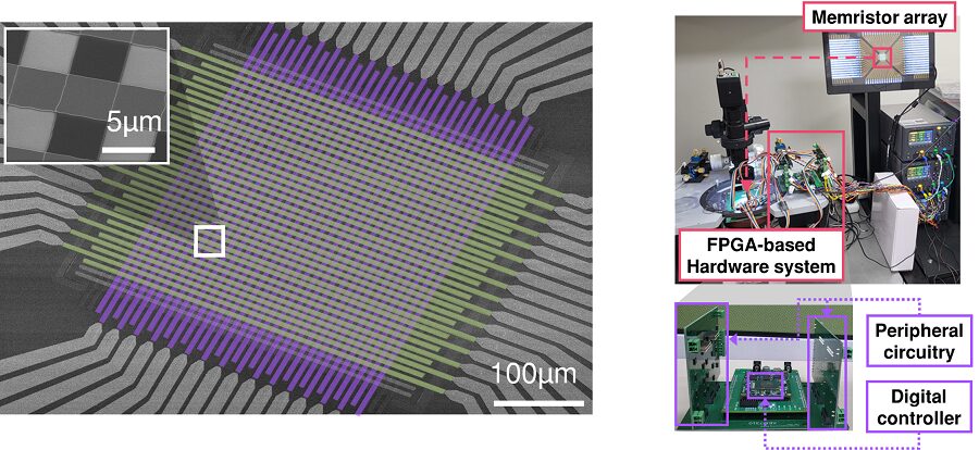
What is special about this computing chip is that it can learn and correct errors that occur due to non-ideal characteristics that were difficult to solve in existing neuromorphic devices. For example, when processing a video stream, the chip learns to automatically separate a moving object from the background, and it becomes better at this task over time.
This self-learning ability has been proven by achieving accuracy comparable to ideal computer simulations in real-time image processing. The research team’s main achievement is that it has completed a system that is both reliable and practical, beyond the development of brain-like components.
The research team has developed the world’s first memristor-based integrated system that can adapt to immediate environmental changes, and has presented an innovative solution that overcomes the limitations of existing technology.
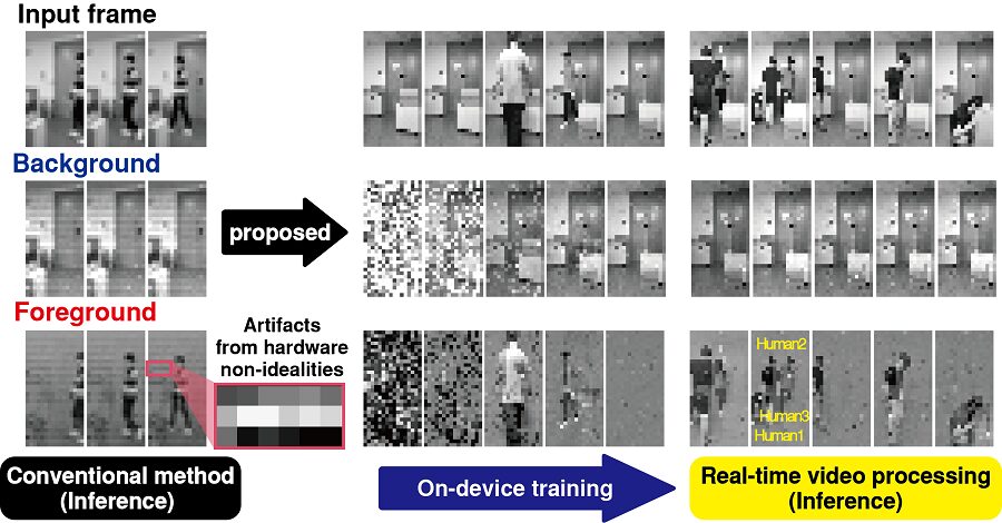
At the heart of this innovation is a next-generation semiconductor device called a memristor*. The variable resistance characteristics of this device can replace the role of synapses in neural networks, and by utilizing it, data storage and computation can be performed simultaneously, just like our brain cells.*Memristor: A compound word of memory and resistor, next-generation electrical device whose resistance value is determined by the amount and direction of charge that has flowed between the two terminals in the past.
The research team designed a highly reliable memristor that can precisely control resistance changes and developed an efficient system that excludes complex compensation processes through self-learning. This study is significant in that it experimentally verified the commercialization possibility of a next-generation neuromorphic semiconductor-based integrated system that supports real-time learning and inference.
This technology will revolutionize the way artificial intelligence is used in everyday devices, allowing AI tasks to be processed locally without relying on remote cloud servers, making them faster, more privacy-protected, and more energy-efficient.
“This system is like a smart workspace where everything is within arm’s reach instead of having to go back and forth between desks and file cabinets,” explained KAIST researchers Hakcheon Jeong and Seungjae Han, who led the development of this technology. “This is similar to the way our brain processes information, where everything is processed efficiently at once at one spot.”
The research was conducted with Hakcheon Jeong and Seungjae Han, the students of Integrated Master’s and Doctoral Program at KAIST School of Electrical Engineering being the co-first authors, the results of which was published online in the international academic journal, Nature Electronics, on January 8, 2025. *Paper title: Self-supervised video processing with self-calibration on an analogue computing platform based on a selector-less memristor array ( https://doi.org/10.1038/s41928-024-01318-6 )
This research was supported by the Next-Generation Intelligent Semiconductor Technology Development Project, Excellent New Researcher Project and PIM AI Semiconductor Core Technology Development Project of the National Research Foundation of Korea, and the Electronics and Telecommunications Research Institute Research and Development Support Project of the Institute of Information & communications Technology Planning & Evaluation.
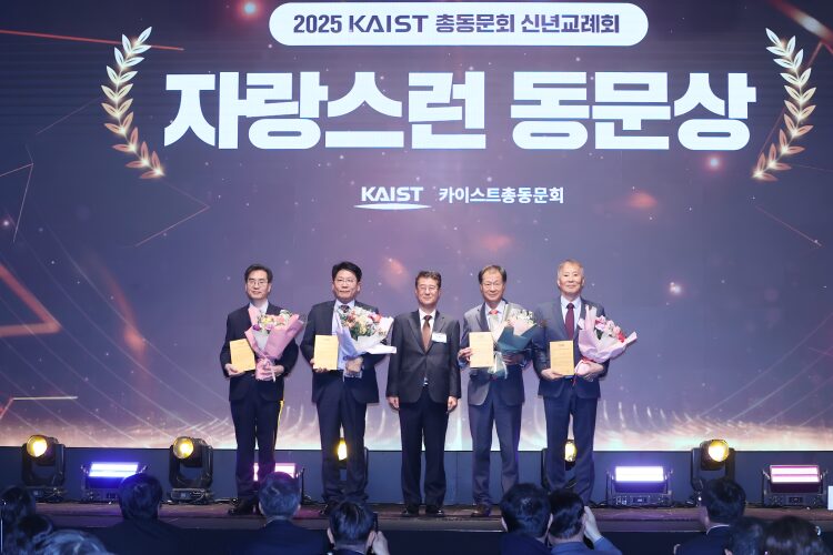
<Professor Myung-Hyun (first from the left) and Jeong-Han, CEO of i3system (fifth from the left)>
EE Professor Hyun Myung (Bachelor’s 1992, Master’s 1994, Ph.D. 1998) and Han Jung, CEO of i3system (Master’s 1991, Ph.D. 1996), both alumni of our department, have been selected as recipients of the ‘Proud Alumni Award’ presented by the KAIST Alumni Association.
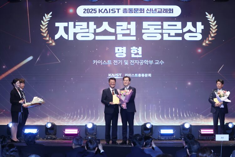
Professor Hyun Myung achieved first place at the Quadruped Robot Challenge (QRC), part of the 2023 IEEE International Conference on Robotics and Automation (ICRA), with his ‘DreamWaQ’ system—a blind walking technology based on deep reinforcement learning. The ‘DreamWalker’ robot leverages this fully autonomous walking technology, which perceives the environment and determines optimal paths. His pioneering work has significantly contributed to enhancing the competitiveness of South Korea’s robotics industry.
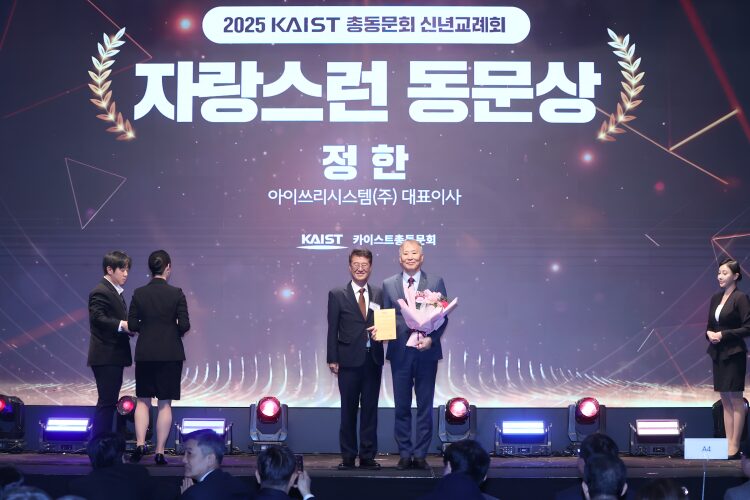
Han Jung, CEO of i3system, is a first-generation researcher in the field of infrared detectors in Korea. Over 30 years, he has developed military detectors and founded i3system Co., Ltd., a specialized infrared detector company, in 1998. The company currently supplies over 80% of infrared detectors used by the South Korean military and has achieved export success in over 20 countries.
The ‘KAIST Proud Alumni Award’ is granted by the KAIST Alumni Association to alumni who have enhanced the university’s reputation through contributions to national and societal development, academic achievements, or community service. Established in 1992, the award has been presented to 126 recipients to date. The selection is based on achievements over the past year, and the award ceremony was held during the 2025 KAIST Alumni Association New Year’s Reception on Friday, January 17, at 5PM at the EL Tower in Seoul.
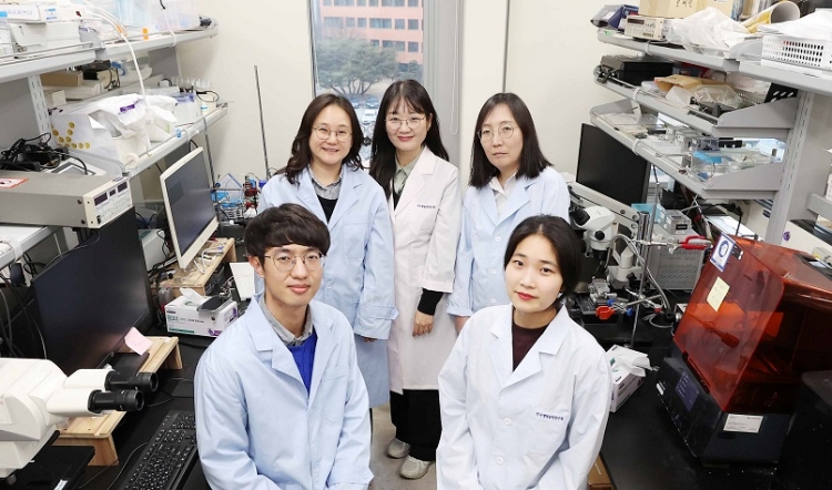
The EE research team led by Professor Hyunjoo J. Lee in collaboration with Dr. Mi-Young Son and Dr. Mi-Ok Lee at Korea Research Institute of and Biotechnology (KRIBB has developed a highly stretchable protruding microelectrode array platform for non-invasive electrophysiological signal measurement of organoids.
Organoids* are highly promising models for human biology and are expected to replace many animal experiments. Their potential applications include disease modeling, drug screening, and personalized medicine as they closely mimic the structure and function of humans. *Organoids: three-dimensional in vitro tissue models derived from human stem cells
Despite these advantages, existing organoid research has primarily focused on genetic analysis, with limited studies on organoid functionality. For effective drug evaluation and precise biological research, technology that preserves the three-dimensional structure of organoids while enabling real-time monitoring of their functions is needed. However, it’s challenging to provide non-invasive ways to evaluate the functionalities without incurring damage to the tissues. This challenge is particularly significant for electrophysiological signal measurement in cardiac and brain organoids since the sensor needs to be in direct contact with organoids of varying size and irregular shape. Achieving tight contact between electrodes and the external surface of the organoids without damaging the organoids has been a persistent challenge.
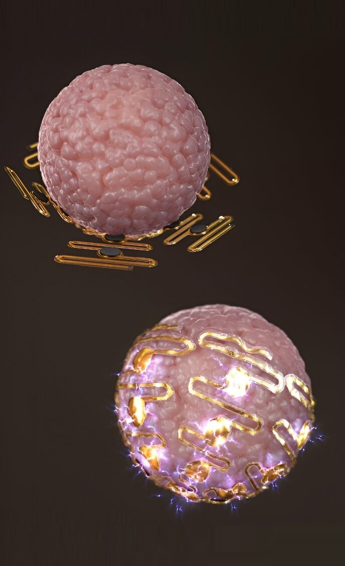
Prof. Hyunjoo J. Lee’s research team developed a highly stretchable microelectrode array with a unique serpentine structure that contacts the surface of organoids in a highly conformal fashion. They successfully demonstrated real-time measurement and analysis of electrophysiological signals from two types of electrogenic organoids (heart and brain). By employing a micro-electromechanical system (MEMS)-based process, the team fabricated the serpentine-structured microelectrode array and used an electrochemical deposition process to develop PEDOT:PSS-based protruding microelectrodes. These innovations demonstrated exceptional stretchability and close surface adherence to various organoid sizes. The protruding microelectrodes improved contact between organoids and the electrodes, ensuring stable and reliable electrophysiological signal measurements with high signal-to-noise ratios (SNR).
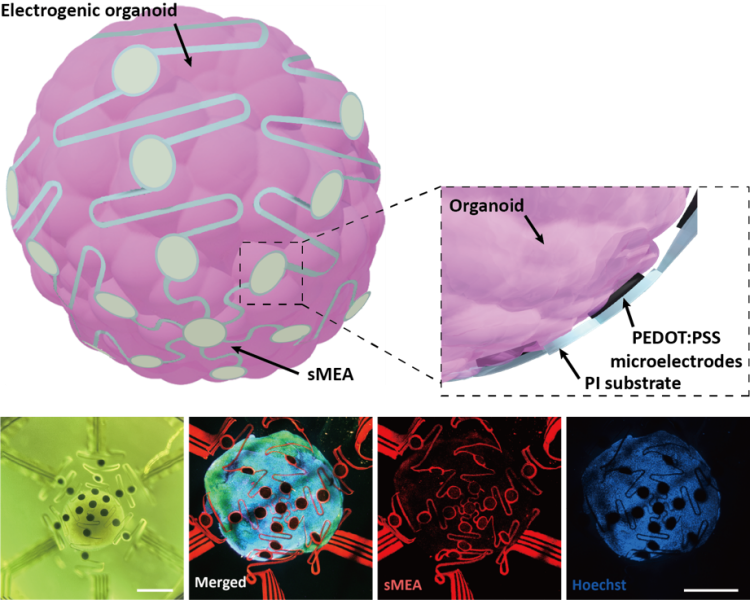
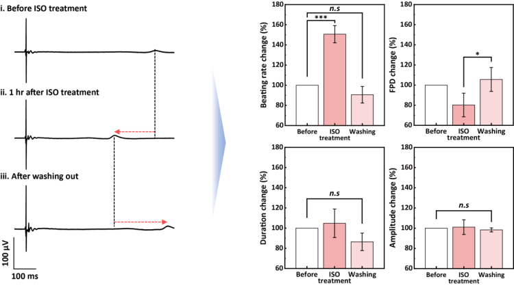
Using this technology, the team successfully monitored and analyzed electrophysiological signals from cardiac spheroids of various sizes, revealing three-dimensional signal propagation patterns and identifying changes in signal characteristics according to size. They also measured electrophysiological signals in midbrain organoids, demonstrating the versatility of the technology. Additionally, they monitored signal modulations induced by various drugs, showcasing the potential of this technology for drug screening applications.
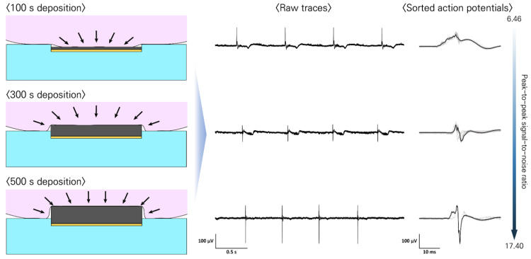
Prof. Hyunjoo Jenny Lee stated, “By integrating MEMS technology and electrochemical deposition techniques, we successfully developed a stretchable microelectrode array adaptable to organoids of diverse sizes and shapes. The high practicality is a major advantage of this system since the fabrication is based on semiconductor fabrication with high volume production, reliability, and accuracy. This technology that enables in situ, real-time analysis of states and functionalities of organoids will be a game changer in high-through drug screening.”
This study led by Ph.D. candidate Kiup Kim from KAIST and Ph.D. candidate Youngsun Lee from KRIBB, with significant contributions from Dr. Kwang Bo Jung, was published online on December 15, 2024 in Advanced Materials (IF: 27.4).
This research was supported by a grant from 3D-TissueChip Based Drug Discovery Platform Technology Development Program (No. 20009209) funded by the Ministry of Trade, Industry & Energy (MOTIE, Korea), by the Commercialization Promotion Agency for R&D Outcomes (COMPA) funded by the Ministry of Science and ICT (MSIT) (RS-2024-00415902), by the K-Brain Project of the National Research Foundation (NRF) funded by the Korean government (MSIT) (RS-2023-00262568), by BK21 FOUR (Connected AI Education & Research Program for Industry and Society Innovation, KAIST EE, No. 4120200113769), and by Korea Research Institute of Bioscience and Biotechnology (KRIBB) Research Initiative Program (KGM4722432).
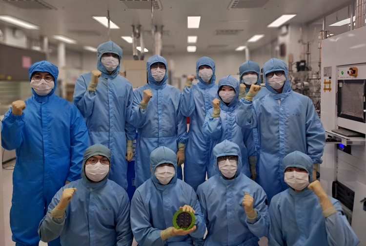
Ferroelectric materials are being highlighted as a key material for the development of next-generation semiconductor technologies due to their characteristic of storing charges well, making them comparable to a “material that remembers electricity.” The KAIST research team has succeeded in developing high-performance, high-density next-generation memory devices that overcome the limitations of DRAM and NAND Flash memory, the two pillars of the current memory semiconductor industry.
EE Professor Sanghun Jeon’s research team has developed next-generation memory and storage memory technology using hafnia-based ferroelectric materials*. *Hafnia-Based Ferroelectric Material: A non-volatile insulating material actively researched as a core material for next-generation semiconductors, with excellent physical properties such as compatibility with CMOS processes, high speed, and durability.
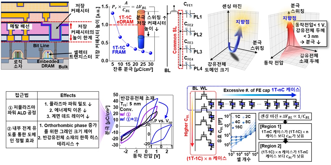
DRAM memory is a type of volatile memory used to store data in devices such as smartphones, computers, and USB drives. Because of its volatile nature, stored data is lost when external power is cut off. However, it has been used as the main memory due to its low manufacturing cost and high integration density. Despite these advantages, as DRAM memory technology advances, the size of memory cells becomes smaller, reducing the capacity of the storage capacitors that store information. This eventually makes it difficult to sustain memory operation.
The research team focused on overcoming the limitations of these storage capacitors to achieve higher storage capacity in physically small areas. To this end, they developed a hafnia-based ferroelectric ultrathin high-k material. The results showed the lowest reported equivalent oxide thickness (EOT) of 2.4 Å (approximately one ten-thousandth the thickness of a human hair) for DRAM capacitors to date.
The team also developed ferroelectric memory (FRAM), which is being considered as a potential replacement for DRAM. This technology ensures non-volatile data storage and erasure even at low voltages below 1V, significantly improving energy efficiency and making it essential for next-generation memory.
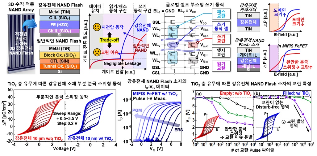
Following advancements in DRAM technology, the team developed next-generation memory technology to overcome the limitations of NAND Flash memory using hafnia-based ferroelectric materials. NAND Flash memory, a non-volatile memory used in devices like smartphones, computers, and USB drives, has evolved to increase storage capacity by stacking multiple layers. However, physical limitations make it challenging to stack more than 500 or 1,000 layers.
In response, the research team applied ferroelectric materials to NAND Flash memory, adding a thin TiO2 interfacial layer to achieve stable data retention in a 3D vertical structure with over 1,000 layers. Furthermore, the team succeeded in developing a high-performance oxide channel-based NAND Flash device, capable of storing more data and maintaining data stability for over 10 years, overcoming the limitations of traditional oxide channel-based memory devices that struggled with complete data erasure.
Professor Jeon stated, “These research results are expected to provide a breakthrough in memory semiconductor technology, which has been stagnant due to scaling issues, and contribute to the commercialization of various AI computing and edge computing technologies in the future.”
Dr. Venkateswarlu Gaddam, PhD candidates Ki-Wook Kim, Hong-Rae Cho, Jung-Hyun Hwang, Sang-Ho Lee, master’s students Hyo-Jun Choi and Hyun-Jun Kang participated as co-first authors. These research achievements were internationally recognized, with five papers presented at top-tier semiconductor industry conferences in 2024 (2 at VLSI 2024, 3 at IEDM 2024).
- “In-depth analysis of the Hafnia ferroelectrics as a key enabler for low voltage & QLC 3D VNAND beyond 1K layers: Experimental demonstration and modeling,” VLSI 2024. DOI: 10.1109/VLSITechnologyandCir46783.2024
- “Low-Damage Processed and High-Pressure Annealed High-k Hafnium Zirconium Oxide Capacitors near Morphotropic Phase Boundary with Record-Low EOT of 2.4 Å & high-k of 70 for DRAM,” VLSI 2024. DOI: 10.1109/VLSITechnologyandCir46783.2024
- “Unveiling the Origin of Disturbance in FeFET and the Potential of Multifunctional TiO2 as a Breakthrough for Disturb-free 3D NAND Cell: Experimental and Modeling,” IEDM 2024.
- “Oxide Channel Ferroelectric NAND Device with Source-Tied Covering Metal Structure: Wide Memory Window (14.3 V), Reliable Retention (> 10 years) and Disturbance Immunity (△Vth ≤ 0.1 V) for QLC Operation,” IEDM 2024.
- “Design Methodology for Low-Voltage Operational (≤1 V) FRAM Cell Capacitors and Approaches for Overcoming Disturb Issues in 1T-nC Arrays: Experimental & Modeling,” IEDM 2024.
IEEE VLSI and IEEE IEDM conferences are considered the “Olympics of semiconductors,” where leading companies like Samsung Electronics, SK Hynix, Micron, and Intel, as well as renowned academics, share the latest technological advancements and discuss future directions.
This research was conducted in collaboration with Samsung Electronics and Hanyang University, supported by the Korea Evaluation Institute of Industrial Technology (KEIT), the Ministry of Science and ICT’s Innovation Research Center (IRC) program, and funding from Samsung Electronics.
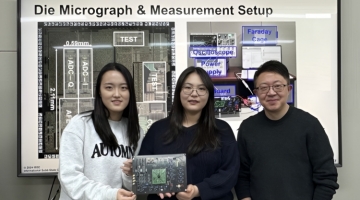
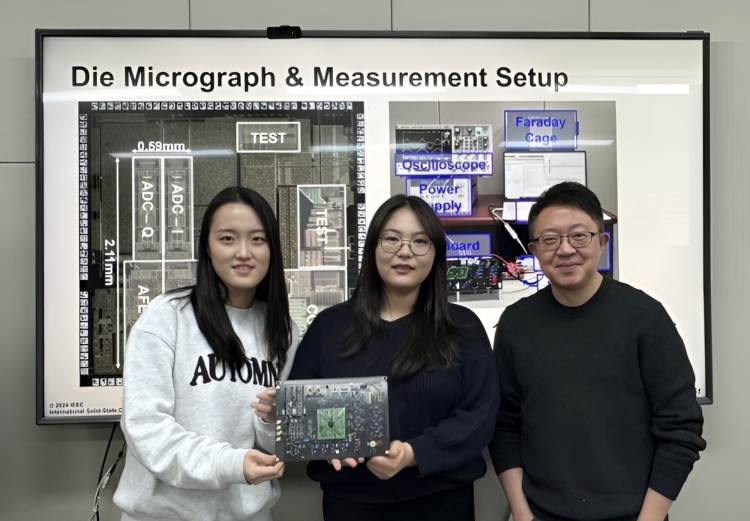
The growing interest in wearable medical devices, which monitor physiological signals to analyze users’ health and predict potential diseases, has fueled advancements in various measurement technologies. One notable example is bio-impedance measurement, widely recognized for providing body composition data through “InBody.” With significant improvements in resolution, this technology can also capture plethysmography, enabling the measurement of heart rate information and further expanding its applications in health monitoring.
Recently, an international research team developed a new method to measure bio-impedance with five times greater resolution than existing technologies, using only two electrodes. This breakthrough, especially significant for the miniaturization of wearable devices, was the result of a collaboration between KAIST’s IMPACT Lab, led by Associate Professor Minkyu Je, and New York University Abu Dhabi (NYUAD), led by Associate Professor Sohmyung Ha.
Compared to the conventional four-electrode system, which is less suitable for compact devices, the two-electrode system offers significant advantages in miniaturization. However, previous two-electrode systems have faced challenges due to baseline impedance interference and increased noise proportional to the measured impedance.
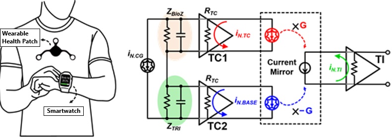
To overcome these limitations, the team developed an innovative semiconductor circuit design that effectively cancels out baseline impedance and associated noise. This design eliminates the need for a separate current generation circuit, reducing power consumption and improving measurement efficiency. The proposed system resolves noise issues caused by impedance phase and magnitude variations, achieving both high resolution and reliability.
“This bio-impedance measurement technology demonstrated up to five times better noise performance compared to conventional methods across various impedance models,” said Associate Professor Minkyu Je, a corresponding author of the work. “We believe this advancement will significantly contribute to the development of personalized health management and disease prediction technologies.”
The results of this work were published in the IEEE Journal of Solid-State Circuits, one of the most prestigious journals in the field of semiconductor integrated circuits and systems. The article, titled “A Bio-Impedance Readout IC With Complex-Domain Noise-Correlated Baseline Cancellation”, was featured in the journal in November 2024.

KAIST Ph.D. candidates Haidam Choi and Song-I Cheon were the co-first authors, while Professors Minkyu Je and Sohmyung Ha served as co-corresponding authors. The research was also presented at the International Solid-State Circuits Conference (ISSCC), the leading global conference in the field.
This work was funded by Korea’s Ministry of Science and ICT as part of projects focusing on continuous musculoskeletal monitoring and rehabilitation technologies, as well as the development of biosignal sensor-based exoskeleton devices and integrated systems.
Research Publication:
IEEE Journal of Solid-State Circuits (2024), DOI:10.1109/JSSC.2024.3439865
Title: A Bio-Impedance Readout IC With Complex-Domain Noise-Correlated Baseline Cancellation