Shinhyun Choi's Research Laboratory [Memristor for AI]

Link: https://www.shinhyunlab.kaist.ac.kr/

Memristor for AI

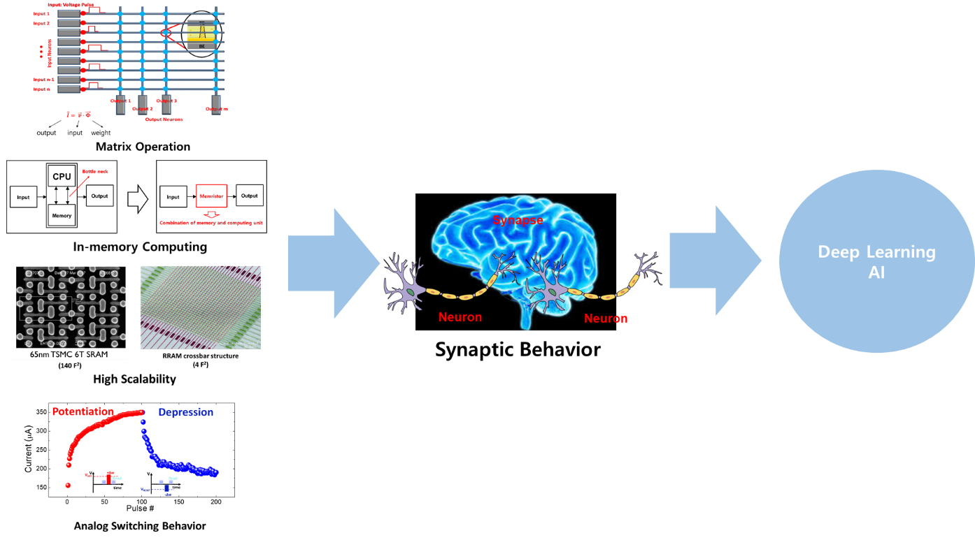
Memristor, also called RRAMs, have attracted tremendous attention as a candidate for machine learning, neuromorphic computing and artificial intelligence. Memristor has two terminals structure, which allows the device to be fabricated into large crossbar array. Moreover, a single memristor has an analog switching behavior unlike conventional devices such as CMOS based processor. Due to these characteristics, effective matrix operation is possible through memristor array, which makes the memristor adequate as a device for deep learning process and artificial intelligence. The inherent memory effect of memristor removes bottlenecks between memory and processor unit, existing on conventional AI processor. Other properties such as high scalability, low power consumption and fast switching speed are the remarkable strength of memristor for AI and deep learning applications.

%EC%B5%9C%EC%8B%A0%ED%98%841

Research area of Emerging Nano Technology and Integrated Systems Lab (ENTIS)

Our lab focuses are 1) to overcome the limitations of conventional memristor and 2) to develop memristor-based platform for various deep neural network(DNN), spiking neural network(SNN) and other applications.

1. Memristor Devices Development

Conventional memristors suffer from unavoidable spatial-temporal variation due to uncontrollable, stochastic filament formation. Our Lab is now developing a new strategy to achieve uniform switching through CMOS compatible materials/fabrication steps as well as linearity, retention and endurance.

%EC%B5%9C%EC%8B%A0%ED%98%842

clip image004

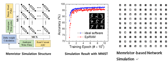
2. Artificial Neural Network Simulation using memristor

To optimize Memristor devices for Artificial Neural Network (ANN) algorithm such as Deep Neural Network (DNN) and Spiking Neural Network (SNN), our Lab is simulating memristor devices arrays using software reflecting hardware conditions.

%EC%B5%9C%EC%85%98%ED%98%843

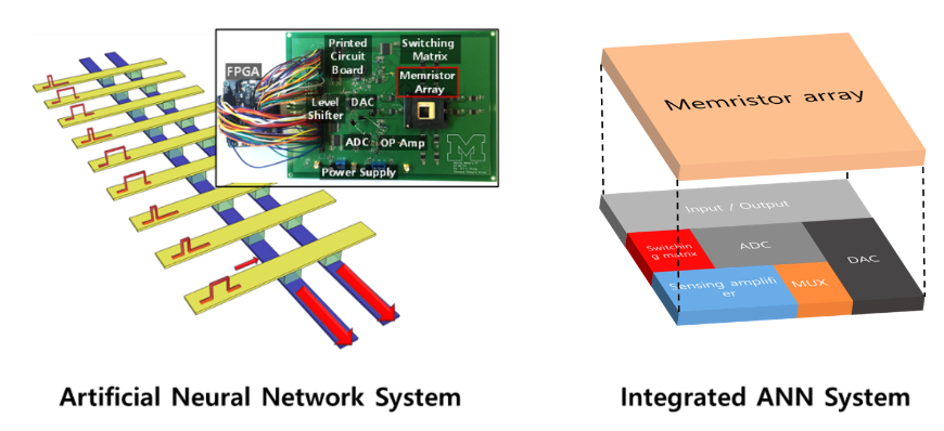
3. Artificial Neural Network System Design and Integration

Our lab designs artificial neural network system on customized PCB board and integrated chip based on memristor device utilized as an AI hardware. The goal is developing large-scale neural network array for AI hardware processing big data. Another aim is integration of the system, broadening the application of memristor-based ANN system.

%EC%B5%9C%EC%8B%A0%ED%98%844

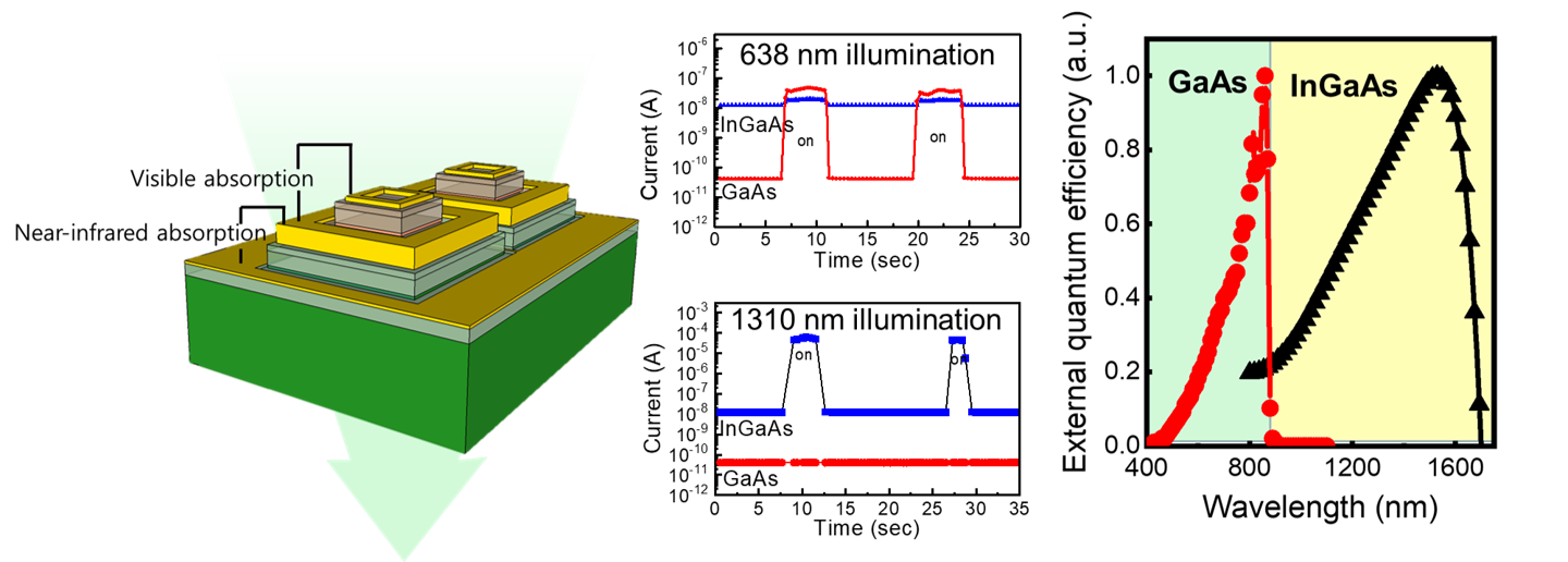
Monolithic integration of GaAs//InGaAs photodetectors for multicolor detection

Prof. Sanghyeon Kim’s paper on the multi-color photodetector, which can be used as a compact photonic sensor for AI chip was presented in VLSI symposia 2019*.

*VLSI symposia is the one of flagship conference in VLSI society.

Title: Monolithic integration of GaAs//InGaAs photodetectors for multicolor detection

Multicolor photodetectors (PDs) by using bulk p-i-n based visible GaAs and near-infrared (IR) InGaAs PD was successfully fabricated via monolithic integration by wafer bonding and epitaxial lift-off. It showed high-performance individual operation comparable to that of bulk PDs with tight vertical alignment on a single substrate for future high-resolution multicolor PDs. At the same time, it covered a broad wavelength range from visible to IR.


7


Figure 1. Multi-Color Photodetector

Large-Scale, Low-Power Nonvolatile Memory Based on Few-Layer MoS2 and Ultrathin Polymer Dielectrics

A research article authored by Sang Cheol Yang (KAIST EE), Junhwan Choi (KAIST CBE), Byung Chul Jang (KAIST EE), Woonggi Hong (KAIST EE), Gi Woong Shim (KAIST EE), Sang Yoon Yang (KAIST EE), Sung Gap Im (KAIST CBE), and Sung‐Yool Choi (KAIST EE; Corresponding author) was published in Advanced Electronic Materials (2019.05)

Article title: Large-Scale, Low-Power Nonvolatile Memory Based on Few-Layer MoS2 and Ultrathin Polymer Dielectrics

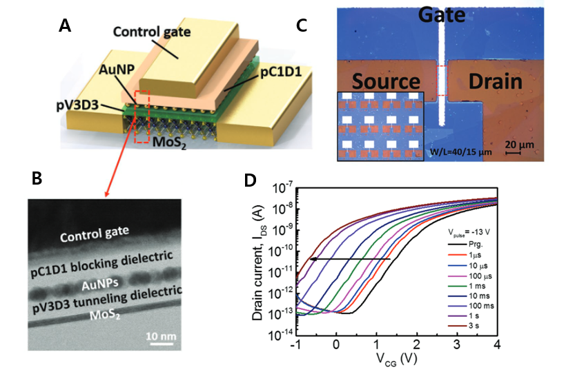
With the advent of artificial intelligence and the Internet of Things, demand has grown for flexible, low-power, high-density nonvolatile memory capable of handling vast amounts of information. Ultrathin-layered 2D semiconductor materials such as molybdenum disulfide (MoS2) have considerable potential for flexible electronic device applications because of their unique physical properties. However, development of flexible MoS2-based flash memory is challenging, as there is a lack of flexible dielectric materials with sufficient insulating properties for use in flash memory devices with dielectric bilayers. Here, large-scale, low-power nonvolatile memory is realized based on a chemical vapor deposition (CVD)-grown millimeter-scale few-layer MoS2 semiconductor channel and polymer dielectrics prepared via an initiated CVD (iCVD) process. Using the outstanding insulating properties and solvent-free nature of iCVD, fabricated memory devices with a tunable memory window, a high on/off ratio (≈106), low operating voltages (≈13 V), stable retention times exceeding 105 s with a possible extrapolated duration of years, and cycling endurance exceeding 1500 cycles are demonstrated. Owing to these characteristics, these devices distinctly outperform previously reported MoS2-based memory devices. Leveraging the inherent mechanical flexibility of both ultrathin polymer dielectrics and MoS2, this work is a step toward realization of large-scale, low-power, flexible MoS2-based flash memory.

%ED%8F%B4%EB%A6%AC%EB%A8%B8

Figure 1. A Schematic illustration of fabricated MoS2-based memory device composed of pV3D3 tunneling dielectric, Au nanoparticle (NP) FG, and pC1D1 blocking dielectric layer. B Cross-sectional HRTEM image of memory device. C Optical microscopy image of fabricated 5 × 6 memory device array. D Transfer curves as functions of pulse width during erasing operation.

A Recoverable Synapse Device Using a Three-Dimensional Silicon Transistor

A research article authored by Jae Hur (KAIST EE), Byung Chul Jang (KAIST EE), Jihun Park (KAIST EE), Dong-Il Moon (KAIST EE), Hagyoul Bae (KAIST EE), Jun-Young Park (KAIST EE), Gun-Hee Kim (KAIST EE), Seung-Bae Jeon (KAIST EE), Myungsoo Seo (KAIST EE), Sungho Kim (KAIST EE), Sung-Yool Choi (KAIST EE; Corresponding author), and Yang-Kyu Choi (KAIST EE; Corresponding author) was published at Advanced Functional Materials (2018.11)

Article title: A Recoverable Synapse Device Using a Three-Dimensional Silicon Transistor

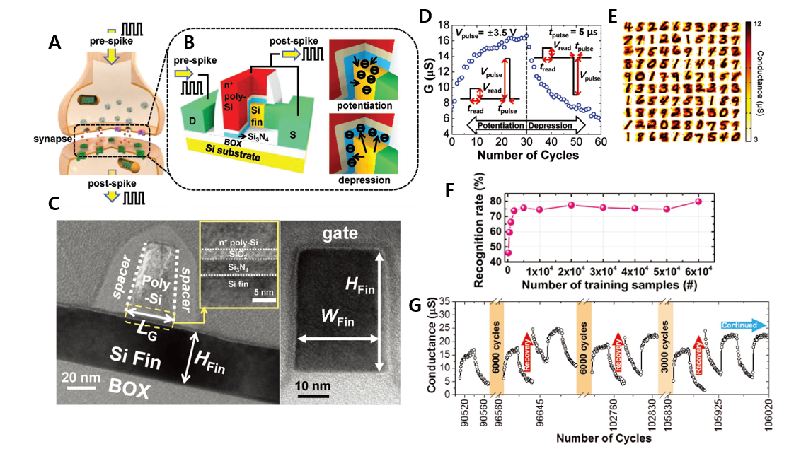
To prepare for the upcoming big-data era, numerous attempts are underway to develop a neuromorphic system which is capable of imitating a biologic neural network. Despite the significant improvements to software-based artificial neural networks (ANNs) recently, they remain inefficient in terms of energy use. Alternatively, many researchers have been attracted to hardware-based ANNs by fundamentally mimicking neural circuits and synapses. In this study, a two-terminal silicon-channel synapse (SINAPSE) with a poly-Si/SiO2/Si3N4 gate stack over a silicon channel is introduced, and demonstrated the smallest size of a synapse device reported thus far, along with reliable, low-power performance. A distinctive feature of SINAPSE is that it emulates synaptic recovery, a retrieval process for neurotransmitters which would be otherwise depleted. By applying an electrical recovery pulse to SINAPSE, synaptic recovery was for the first time successfully imitated. Experimental results demonstrate the potential of the curable SINAPSE as a fundamental unit in neuromorphic circuitry.

%ED%9A%8C%EB%B3%B5%EA%B0%80%EB%8A%A5%20%EC%8B%9C%EB%83%85%EC%8A%A4

Figure 1. A A schematic illustration of a synapse between a presynaptic and postsynaptic neuron in a biological system. B A schematic of the SINAPSE structure and the electron trajectories during the potentiation and depression processes of the charge-trap nitride of SINAPSE. C Cross-sectional TEM images of SINAPSE along the silicon nanowire direction (left-side panel) and along the gate direction (right-side panel). D Analog conductance modulation behavior of SINAPSE as a function of the number of applied pulse cycles. (Inset) Applied presynaptic voltage schemes for potentiation and depression. E Learned weights map with the ANN, which is based on a SINAPSE device with 100 output neurons. F Recognition rate as a function of the number of the number of training instances. G Recovery (Vpulse = 6 V and tpulse = 1 ms) results for SINAPSE after fatigue.

Zero-static-power nonvolatile logic-in-memory circuits for flexible electronics

A research article authored by Byung Chul Jang (KAIST EE), Sang Yoon Yang (KAIST EE), Hyejeong Seong (KAIST CBE), Sung Kyu Kim (KAIST MSE), Junhwan Choi (KAIST CBE), Sung Gap Im (KAIST CBE), and Sung-Yool Choi (KAIST EE; Corresponding author) was published at Nano Research (2017.07)

Article title: Zero-static-power nonvolatile logic-in-memory circuits for flexible electronics

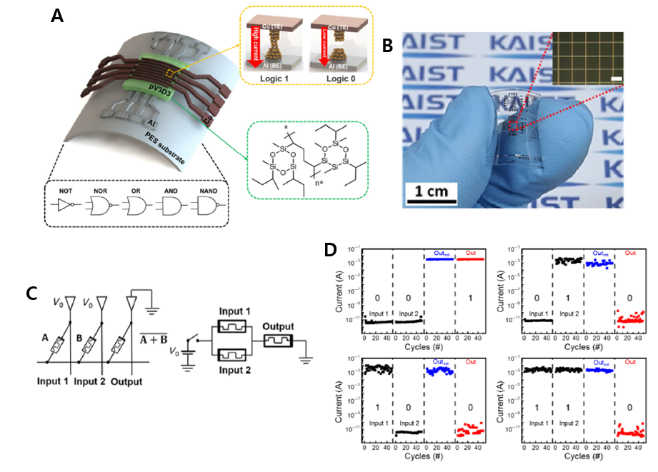
Flexible logic circuits and memory with ultra-low static power consumption are in great demand for battery-powered flexible electronic systems. Here, we show that a flexible nonvolatile logic-in-memory circuit enabling normally-off computing can be implemented using a poly(1,3,5-trivinyl-1,3,5-trimethyl cyclotrisiloxane) (pV3D3)-based memristor array. Although memristive logic-in-memory circuits have been previously reported, the requirements of additional components and the large variation of memristors have limited demonstrations to simple gates within a few operation cycles on rigid substrates only. Using memristor-aided logic (MAGIC) architecture requiring only memristors and pV3D3-memristor with good uniformity on a flexible substrate, for the first time, we experimentally demonstrated our implementation of MAGIC-NOT and -NOR gates during multiple cycles and even under bent conditions. Other functions, such as OR, AND, NAND, and a half adder, are also realized by combinations of NOT and NOR gates within a crossbar array. This research advances the development of novel computing architecture with zero static power consumption for battery-powered flexible electronic systems.

Zero%20static

Figure 1. A Schematic illustration of a pV3D3-memristor with an 8 × 8 crossbar array on a plastic substrate. The inset with the orange dotted line shows the logical states of the pV3D3-memristor, the inset with the green dotted line shows the molecular structure of pV3D3, and the inset with the black dotted line depicts the feasible logic gates using the pV3D3-memristor. B Photograph of a flexible pV3D3-memristor on a PES substrate. The inset shows a magnified optical image of the flexible pV3D3-memristor array (scale bar: 20 μm). C MAGIC-NOR gate within the crossbar array and its equivalent circuit. D Experimental results of the MAGIC-NOR gate for all input memristor combinations during 50 cycles.

이현주 교수, 머신러닝 기반 치매연구 관련 전자신문 보도

이현주교수가 지난 18일 전자신문에 보도되었습니다. 뇌파를 측정하여 수집한 뇌전도 데이터셋(EEG)을 머신러닝으로 학습하고 이를 기반으로 퇴행성 뇌 환자의 뇌를 자극하여 치료, 완화시키는 연구로 소개되었습니다.

기사 Link: http://www.etnews.com/20170616000183 KAIST, AI·IoT 기술로 퇴행성 뇌질환 정복 나서