Highlights


From smartphones to large-scale AI servers, most digital information in modern society is stored in NAND flash memory*. EE researchers have developed an innovative technology that can overcome the limitations of next-generation semiconductors, where more data must be stored in smaller spaces. This advancement is expected to serve as a key enabling technology for realizing ultra-high-capacity memory.
* NAND flash memory: a non-volatile semiconductor memory used in storage devices such as smartphones and SSDs, where data such as photos, videos, and apps are retained even when power is turned off.
A research team led by Professor Byung Jin Cho of the School of Electrical Engineering has overcome the scaling limitations of 3D V-NAND memory by implementing a “smart gate” structure that selectively controls electron movement depending on conditions, using a new material applied to an ultra-thin semiconductor layer thinner than a human hair.
*3D V-NAND: a memory technology that stacks memory cells vertically, unlike conventional planar (2D) arrangements, enabling higher data storage density.
This research is particularly significant in that it addresses the longstanding issues of speed degradation and reliability during data write and erase operations by utilizing a novel material called boron oxynitride (BON).
In semiconductor memory, the tunneling layer—a thin insulating layer that acts as a pathway for electrons to move in and out of the memory cell—has historically faced a trade-off between performance and reliability.
With conventional materials, it has been difficult to achieve both simultaneously. For example, the widely used silicon oxynitride (SiON) increases data leakage when the tunneling path is widened to improve erase speed, while narrowing the path to prevent leakage significantly slows down data erasure. This trade-off has been a major obstacle to implementing next-generation penta-level cell (PLC) technology.
PLC technology stores 5 bits of data per memory cell by distinguishing 32 different voltage states, allowing much higher data density within the same physical size.
To overcome this limitation, the research team introduced BON, a completely new material beyond conventional silicon-based systems, into the tunneling layer. This material exhibits a unique physical property in which the energy barrier height differs depending on the type of charge carrier.
Leveraging this property, the team designed an asymmetric energy barrier structure that allows holes (positive charge carriers)—needed for data erase—to pass through easily, while blocking electrons, which represent stored data, from leaking out.
An asymmetric energy barrier refers to a structure in which the energy required for charge carriers to move varies depending on the type of charge. This enables efficient charge transport during erase operations while effectively preventing data loss. The concept is analogous to a “smart gate” that opens easily for entry but firmly blocks exit, implemented at the semiconductor level.
Experimental results showed that devices using the BON tunneling layer achieved up to a 23-fold improvement in erase speed compared to conventional technologies and demonstrated excellent durability with minimal performance degradation even after tens of thousands of operation cycles.
Notably, even under the highly demanding PLC operation—where 32 distinct voltage levels must be precisely controlled—the researchers achieved more than threefold improvement in controlling data distribution across devices.

This achievement is considered by both academia and industry to be beyond a purely experimental result, reaching a level immediately applicable to real semiconductor manufacturing processes.
Professor Byung Jin Cho stated, “This research presents a novel technology that can be directly applied to the production of next-generation ultra-high-capacity memory,” adding, “It will significantly contribute to maintaining Korea’s technological leadership in the semiconductor industry.”
This study was implemented by Dae Hyun Kang, an integrated master’s–PhD student in Electrical Engineering, as the first author. The research was presented at the IEEE International Electron Devices Meeting (IEDM) on December 9, one of the most prestigious conferences in the semiconductor field, attracting global attention.
The work also received the Grand Prize (first place overall in the university category) at the 32nd Samsung Human Tech Paper Awards, marking a notable achievement as a traditional semiconductor device study in a competition typically dominated by AI-related research.
※ Paper title: “Bandgap-Engineered Boron Oxynitride Tunneling Layer for Reliable PLC Operation of 3D V-NAND Flash Memory Devices,” DOI: https://doi.org/10.1109/IEDM50572.2025.11353681
This research was supported by the National Semiconductor Research Lab Core Technology Development Program funded by the Ministry of Science and ICT.


Professor Hyun Myung’s research team from our school received the Deputy Prime Minister and Minister of Science and ICT Award after their study titled “Development of a Small Quadrupedal Robot and Reinforcement Learning-based Control Technology” was selected as the top research project in the engineering field at the Science Gifted R&E Presentation Contest.
The study was conducted over one year in collaboration with Korea Science Academy students So-Min Lee, Jae-Wook Jung, and Han-Sun Cho, and won the Grand Prize at the Korea Science Academy R&E Presentation Contest. Based on this achievement, the team represented Korea Science Academy at the Science Gifted R&E Presentation Contest hosted by the Korea Foundation for Science and Creativity in December 2025, where they achieved this recognition.
Professor Hyun Myung, who supervised the study, also received the Advisor Award (Deputy Prime Minister and Minister of Science and ICT Award).
![[Announcement] 2026 Spring Semester Colloquium Series 4 260311 4](https://ee.kaist.ac.kr/wp-content/uploads/2026/03/260311-4.jpg)
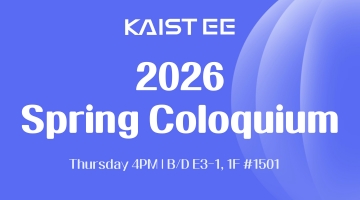
The Spring 2026 Colloquium Series of the KAIST School of Electrical Engineering began on March 12, 2026.
The first speaker, Jihoon Kim, Chief Research Officer of FuriosaAI, delivered a talk titled “Unlock Furiosa RNGD’s Full Potential with Kernel Programming.” In his lecture, he introduced how the dataflow-based architecture of Furiosa RNGD and its kernel programming model enable developers to directly control hardware, making it possible to build high-performance AI inference infrastructure that overcomes the limitations of conventional GPUs. The talk drew significant interest from the audience.
Upcoming lectures will include talks on quantum computing systems by Director Kihwan Kim of the Institute for Basic Science (IBS) (Center for Trapped Ion Quantum Science) and Professor Hui Khoon Ng of the National University of Singapore. In addition, Samsung Display and Samsung Electronics executives Cheol Lae Roh, Jungbae Lee, and Huiwon Je will be invited to discuss technological innovation and industrial applications in AI driven innovation in display manufacturing, AI driven by semiconductor technology and next-generation communications (6G), respectively.
According to Professor Minkyu Je, who organizes the colloquium series, the program will also feature lectures by Prof. Youngjoo Lee, a recently appointed faculty member of the School of EE as well as Prof. Jooyoung Kim, a faculty member involved in entrepreneurship. He encouraged active participation from both students and faculty.
The colloquium lectures are held Thursday at 4:00 PM in Lecture Halls 1 of the Information and Electronics Building (E3-1).


Blood flow is a vital signal of life. When this flow slows down or becomes unstable, it can lead to cardiovascular diseases and shock. However, accurately measuring blood flow has traditionally required hospital equipment. Prof. Kyeongha Kwon’s research team at the School of Electrical Engineering has developed a wireless electronic patch that can measure blood flow in real time simply by attaching it to the skin.
The wireless wearable blood flow monitoring system developed by Prof. Kwon’s team combines deep learning (AI) with multilayer thermal sensing technology. This device can simultaneously measure blood flow velocity and blood vessel depth without directly contacting the vessels (a non-invasive method). Because sensor signals vary depending on how deeply the blood vessels are located beneath the skin, depth information is a key variable for accurately calculating blood flow.
Previously, ultrasound or optical methods were mainly used, but these approaches had limitations, as the equipment was large or the accuracy decreased depending on vessel depth. To overcome these limitations, the research team focused on the fact that when blood flows, subtle heat transfer occurs in the surrounding tissue.

The team developed a “multilayer thermal sensing” technology that analyzes heat transfer pathways three-dimensionally by placing temperature sensors at different depths. By applying AI algorithms, they succeeded in separating and extracting both the depth of blood vessels and the actual blood flow velocity in real time from complex body temperature distributions. Through AI-based analysis, the system can accurately distinguish between vascular depth and actual blood flow velocity within complex temperature patterns of the body.
Experimental results showed that the system successfully measured blood flow velocities in the range of 1–10 mm/s with an error within 0.12 mm/s, and blood vessel depths in the range of 1–2 mm with an error within 0.07 mm. This level of error is smaller than the thickness of a human hair and represents a degree of precision that is difficult to achieve with typical wearable devices.

In particular, when this technology is combined with photoplethysmography (PPG) sensors used in smartwatches, the error in blood pressure measurement can be reduced by up to 72.6%. This indicates that smartwatch-based blood pressure measurements could become much closer to those obtained with hospital equipment. In other words, this achievement can significantly improve the reliability of wearable devices.
This electronic patch can be used in emergency medical settings to detect changes in a patient’s condition in real time. It may also be applied to personalized health management for patients with hypertension or diabetes and to the early detection of acute warning signs such as shock.

Prof. Kyeongha Kwon stated, “This technology provides a fundamental platform for measuring blood flow and blood pressure more accurately, and when combined with smartwatches, it will elevate the level of everyday health monitoring.”
The study was led by Young Min Sim, an integrated M.S.–Ph.D. student, as the first author. The research results were published on February 6 in the world-renowned journal Science Advances.
Paper title: Deep learning–integrated multilayer thermal gradient sensing platform for real-time blood flow monitoring
DOI: 10.1126/sciadv.aea8902
Meanwhile, this research was supported by the Samsung Advanced Institute of Technology (SAIT), the National Research Foundation of Korea (NRF) Outstanding Young Researcher Program (2022R1C1C1010555), the Regional Innovation Leading Research Center (2020R1A5A8018367), the BK21 FOUR Program, and the Artificial Intelligence Semiconductor Graduate School program funded by the Institute of Information & Communications Technology Planning & Evaluation (IITP).


Shilong Zhang, a Ph.D. candidate from Professor Youngsoo Shin’s research group (DT Lab) in the School of Electrical Engineering, has been selected as the recipient of the 2026 SPIE Nick Cobb Memorial Scholarship, receiving a $10,000 award.
The SPIE Nick Cobb Memorial Scholarship is awarded to an outstanding graduate student studying advanced lithography or a related field, jointly funded by Siemens EDA and SPIE. Nick Cobb was a Senior Member of SPIE and Chief Engineer at Mentor Graphics (now Siemens EDA), whose pioneering contributions enabled optical and process proximity correction (OPC) for IC manufacturing.
Zhang has been recognized for his outstanding research accomplishments, including winning the First Place Photronics Best Student Presentation Award at SPIE Photomask Technology + EUV Lithography 2025 and the ISE President Best Paper Award at the 2024 International SoC Design Conference. He was honored during the 2026 SPIE Advanced Lithography + Patterning conference, held February 22–26 in San Jose, California, where he also presented his paper titled “Etch proximity correction for curvilinear layout: Curve sampling with ML etch bias model.”
For details, refer to the link below:
https://spie.org/news/2026-spie-nick-cobb-memorial-scholarship-recipient-announced


Dr. Dongheon Lee from Professor Jung-Woo Choi’s research group will be appointed as an Assistant Professor in the Division of Electronic, Information and Communication Engineering at Pukyong National University, effective September 2026.
Dr. Lee earned his Ph.D. in February 2025, dedicating his research to artificial intelligence models for spatial acoustic analysis. During his doctoral studies, he conducted in-depth research on an integrated acoustic analysis system encompassing speech enhancement, sound source separation, noise reduction, direction-of-arrival estimation, and classification, utilizing spatial acoustic signals collected through multi-channel microphones.
In particular, he presented the “DeepASA” model at NeurIPS 2025, a unified spatial acoustic AI framework capable of comprehensively inferring all related tasks within a single model. In addition, he developed innovative multi-channel speech enhancement models and achieved outstanding research accomplishments by publishing a total of 12 first-author papers in leading conferences and journals in speech and audio, including ICASSP, INTERSPEECH, and IEEE Transactions on Audio, Speech, and Language Processing (TASLP). Furthermore, he demonstrated his practical technological expertise by leading his team to victory in DCASE Task 4, the 2025 international challenge on acoustic scene analysis.
We sincerely congratulate Dr. Dongheon Lee as he embarks on his career as an independent researcher. We wish him continued success in advancing the field of acoustic artificial intelligence and in emerging as a leading scholar in world-class research.


Dr. Kyeongwon Jeong, Dr. Yoontae Jung, and Dr. Edward Jongyoon Choi, Ph.D. graduates from Prof. Minkyu Je’s research group, have been appointed as Assistant Professors at the School of Integrated Technology, Yonsei University; the Department of Semiconductor Engineering, Kyung Hee University; and the Division of Electronic and Semiconductor Engineering, Ewha Womans University, respectively.
Dr. Kyeongwon Jeong received his Ph.D. in February 2023 and subsequently worked as a postdoctoral researcher at ETH Zurich and IBM Research in Zurich, Switzerland. His research focuses on mixed-signal circuit design and intelligent sensor interfaces, including ADCs, neural and ultrasound systems, in-memory computing hardware accelerators, and Ising machine architectures.
Dr. Yoontae Jung earned his B.S., M.S., and Ph.D. degrees (2024) from KAIST. Since 2024, he has been conducting research on neural interface ICs at imec in Leuven, Belgium. His research interests include biomedical ICs, neural ICs, sensor interface ICs for physical AI, and processing-in-memory (PIM) technologies.
Dr. Edward Jongyoon Choi received his Ph.D. in February 2025 and subsequently joined Annapurna Labs (Amazon Web Services) in Silicon Valley as a Circuit Design Engineer, where he contributed to the design of the AWS Trainium accelerator. His primary research interests include AI/ML accelerator design, algorithm–hardware co-design, and processing-in-memory circuit design, with a focus on circuit and architecture design for high-performance, low-power intelligent semiconductor systems.
We look forward to their continued contributions to academia through excellence in research and education and to their impact on the advancement of semiconductor and advanced engineering research worldwide.


Gichan Yun, a Ph.D. candidate from the research group of Prof. Minkyu Je in the School of Electrical Engineering, has been selected as a recipient of the 2025–2026 IEEE Solid-State Circuits Society (SSCS) Predoctoral Achievement Award.
The SSCS Predoctoral Achievement Award is a prestigious program presented to outstanding Ph.D. students worldwide who have demonstrated exceptional research accomplishments in solid-state circuits and systems. Each year, only a limited number of students are selected; this year, Gichan Yun was named among just 30 awardees globally.
Gichan Yun has published a total of 23 international papers, including two ISSCC papers as first author or co–first author. Among these, 17 papers have been published in SSCS-sponsored journals and conferences. His contributions to low-power, high-resolution sensor interface design and his strong academic achievements were key factors leading to this distinguished recognition.


