to be the world’s
top IT powerhouse.We thrive to be the world’s top IT powerhouse.
Our mission is to lead innovations
in information technology, create lasting impact,
and educate next-generation leaders of the world.
- 1
- 6
to be the world’s
top IT powerhouse.We thrive to be the world’s top IT powerhouse.
Our mission is to lead innovations
in information technology, create lasting impact,
and educate next-generation leaders of the world.
- 2
- 6
to be the world’s
top IT powerhouse.We thrive to be the world’s top IT powerhouse.
Our mission is to lead innovations
in information technology, create lasting impact,
and educate next-generation leaders of the world.
- 3
- 6
to be the world’s
top IT powerhouse.We thrive to be the world’s top IT powerhouse.
Our mission is to lead innovations
in information technology, create lasting impact,
and educate next-generation leaders of the world.
- 4
- 6
to be the world’s
top IT powerhouse.We thrive to be the world’s top IT powerhouse.
Our mission is to lead innovations
in information technology, create lasting impact,
and educate next-generation leaders of the world.
- 5
- 6
are a key thrust
in EE researchAI and machine learning are a key thrust in EE research
AI/machine learning efforts are already a big part of ongoing
research in all 6 divisions - Computer, Communication, Signal,
Wave, Circuit and Device - of KAIST EE
- 6
- 6
Jae-Woong Jeong’s
Team Develops
Phase-Change Metal Ink
Kyeongha Kwon’s Team
Enables Battery-Free
CO₂ Monitoring
Yongdae Kim · Insu Yun’s
Team Uncovers
Risks in Mandatory
KSA Tools
Wins Global Robotics Challenge
Hyunchul Shim’s Team
Wins 3rd Place
at A2RL Autonomous
Drone Racing Competition
develops a simulation
framework called vTrain
Achieves Human-Level Tactile Sensing with
Breakthrough Pressure Sensor
Seungwon Shin’s Team
Validates Cyber Risks
of LLMs
Wearable Carbon Dioxide Sensor
Highlights
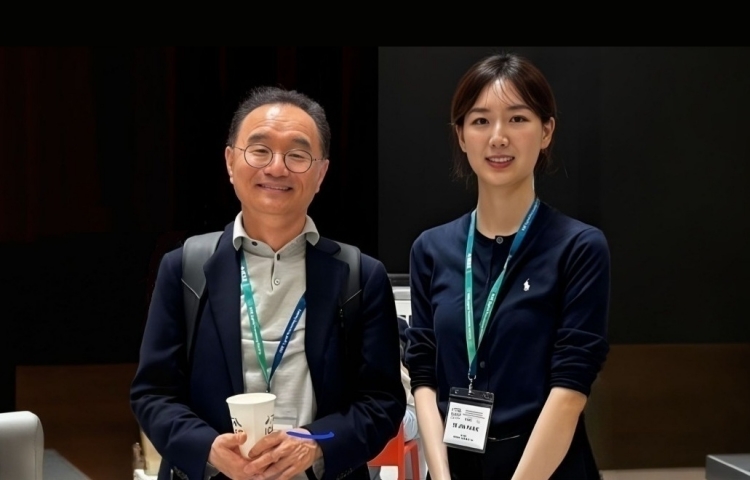
Recently, Spoken Language Models (SLMs) have been spotlighted as next-generation technology that surpasses the limitations of text-based language models by learning human speech without text to understand and generate linguistic and non-linguistic information. However, existing models showed significant limitations in generating long-duration content required for podcasts, audiobooks, and voice assistants. Now, KAIST researcher has succeeded in overcoming these limitations by developing ‘SpeechSSM,’ which enables consistent and natural speech generation without time constraints.
Ph.D. candidate Sejin Park from Professor Yong Man Ro’s research team in the School of Electrical Engineering has developed ‘SpeechSSM,’ a spoken language model capable of generating long-duration speech.

A major advantage of Spoken Language Models (SLMs) is their ability to directly process speech without intermediate text conversion, leveraging the unique acoustic characteristics of human speakers, allowing for the rapid generation of high-quality speech even in large-scale models.
However, existing models faced difficulties in maintaining semantic and speaker consistency for long-duration speech due to increased ‘speech token resolution’ and memory consumption when capturing very detailed information by breaking down speech into fine fragments.
To solve this problem, Se Jin Park developed ‘SpeechSSM,’ a spoken language model using a Hybrid State-Space Model, designed to efficiently process and generate long speech sequences.
This model employs a ‘hybrid structure’ that alternately places ‘attention layers’ focusing on recent information and ‘recurrent layers’ that remember the overall narrative flow (long-term context). This allows the story to flow smoothly without losing coherence even when generating speech for a long time. Furthermore, memory usage and computational load do not increase sharply with input length, enabling stable and efficient learning and the generation of long-duration speech.
SpeechSSM effectively processes unbounded speech sequences by dividing speech data into short, fixed units (windows), processing each unit independently, and then combining them to create long speech.
Additionally, in the speech generation phase, it uses a ‘Non-Autoregressive’ audio synthesis model (SoundStorm), which rapidly generates multiple parts at once instead of slowly creating one character or one word at a time, enabling the fast generation of high-quality speech.
While existing models typically evaluated short speech models of about 10 seconds, Se Jin Park created new evaluation tasks for speech generation based on their self-built benchmark dataset, ‘LibriSpeech-Long,’ capable of generating up to 16 minutes of speech.
Compared to PPL (Perplexity), an existing speech model evaluation metric that only indicates grammatical correctness, she proposed new evaluation metrics such as ‘SC-L (semantic coherence over time)’ to assess content coherence over time, and ‘N-MOS-T (naturalness mean opinion score over time)’ to evaluate naturalness over time, enabling more effective and precise evaluation.
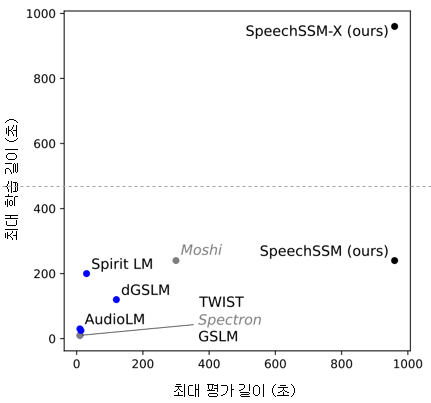
Whereas conventional SLMs have been trained and evaluated on sequences up to 200 seconds in length, SpeechSSM is capable of training and evaluating speech up to 16 minutes. While the proposed model can theoretically generate speech of infinite length with constant memory usage, the experiments were limited to 16 minutes for evaluation purposes.>
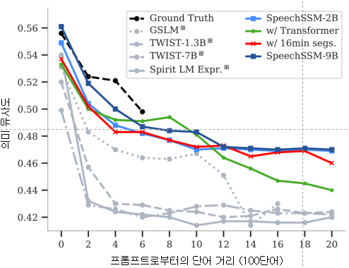
Through these new evaluations, it was confirmed that speech generated by the SpeechSSM spoken language model consistently featured specific individuals mentioned in the initial prompt, and new characters and events unfolded naturally and contextually consistently, despite long-duration generation. This contrasts sharply with existing models, which tended to easily lose their topic and exhibit repetition during long-duration generation.
PhD candidate Sejin Park explained, “Existing spoken language models had limitations in long-duration generation, so our goal was to develop a spoken language model capable of generating long-duration speech for actual human use.” She added, “This research achievement is expected to greatly contribute to various types of voice content creation and voice AI fields like voice assistants, by maintaining consistent content in long contexts and responding more efficiently and quickly in real time than existing methods.”
This research, with Se Jin Park as the first author, was conducted in collaboration with Google DeepMind and is scheduled to be presented as an oral presentation at ICML (International Conference on Machine Learning) 2025 on July 16th.
- Paper Title: Long-Form Speech Generation with Spoken Language Models
- DOI: 10.48550/arXiv.2412.18603
Ph.D. candidate Se Jin Park has demonstrated outstanding research capabilities as a member of Professor Yong Man Ro’s MLLM (multimodal large language model) research team, through her work integrating vision, speech, and language. Her achievements include a spotlight paper presentation at 2024 CVPR (Computer Vision and Pattern Recognition) and an Outstanding Paper Award at 2024 ACL (Association for Computational Linguistics).
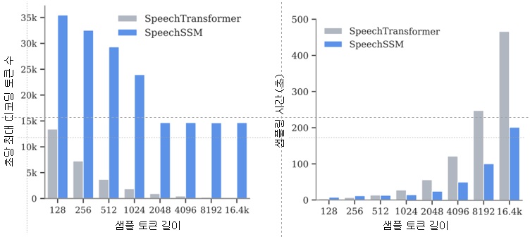
For more information, you can refer to the publication and accompanying demo: SpeechSSM Publications.


Three Ph.D. students from EE—Kyeongha Rho (advisor: Joon Son Chung), Seokjun Park (advisor: Jinseok Choi), and Juntaek Lim (advisor: Minsoo Rhu)—have been selected as recipients of the 2nd Presidential Science Scholarship for Graduate Students.
Kyeongha Rho is conducting research on multimodal self-supervised learning, as well as multimodal perception and generation models. Seokjun Park is currently researching optimization techniques for low-power beamforming in satellite and multi-access systems for next-generation 6G wireless communications, as well as predictive beamforming utilizing artificial intelligence in integrated sensing and communication (ISAC) systems. Juntaek Lim focuses on developing high-performance, secure computing systems by integrating security across both hardware and software.
The Presidential Science Scholarship for Graduate Students is a new initiative launched last year by the Korea Student Aid Foundation to foster world-class research talent in science and engineering. Final awardees receive a certificate of scholarship in the name of the President, along with financial support—KRW 1.5 million per month (KRW 18 million annually) for master’s students and KRW 2 million per month (KRW 24 million annually) for Ph.D. students.
This year’s selection process for the scholarship was highly competitive, with 2,355 applicants vying for 120 spots, resulting in a competition ratio of approximately 20:1.
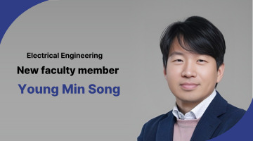
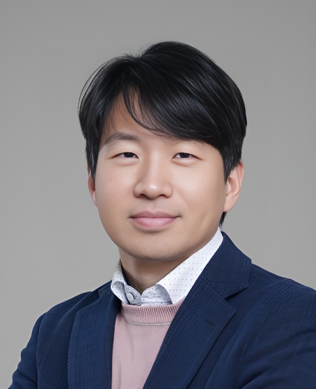
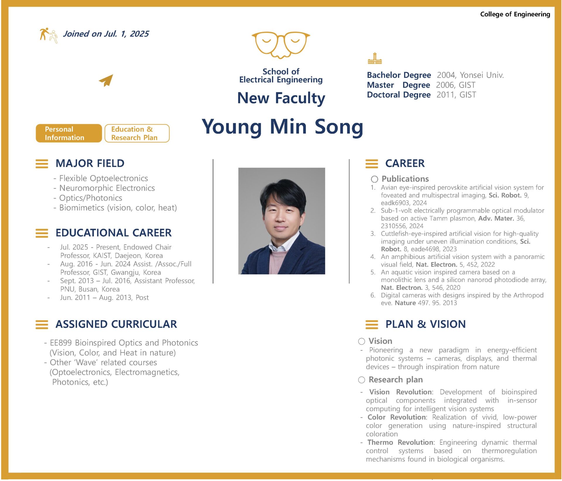
We are pleased to announce that Professor Young Min Song will be joining the KAIST School of Electrical Engineering as of July 1, 2025. Congratulations!
Professor Song’s temporary office is located in Room 1410, Saenel-dong (E3-4). His primary research areas include flexible optoelectronic devices and nanophotonics. He is actively working on biomimetic cameras for intelligent robotics, opto-neuromorphic devices and systems, nanophotonics-based reflective displays, and radiative cooling devices through infrared control. For more details on his research, please visit his homepage.
Homepage: https://www.ymsong.net
Click here to read Professor Song’s recent interview in Nature
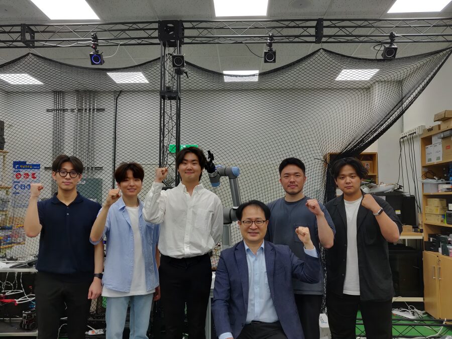
‘Team ACE’ from Professor Dong Eui Cang’s lab in our department achieved outstanding results by winning a Third Prize at the ‘Hugging Face LeRobot Worldwide Hackathon’, held over three days from June 14 to 16.
Composed of Seokjoon Kwon (Master’s Program, Team Leader), Hee-Deok Jang (Ph.D. Program), Hojun Kwon (Master’s Program), Guining Pertin (Master’s Program), and Kyeongdon Lee (Master’s Program) from Professor Dong Eui Chang’s lab, ‘Team ACE’ developed a VLA-based collaborative robot object transfer system and placed 20th out of more than 600 teams worldwide, earning a Third Prize (awarded to teams ranked 6th-24th). In addition, the team also received the KIRIA President’s Award (awarded by the Korea Institute for Robot Industry Advancement) from the local organizing committee in Daegu, South Korea.
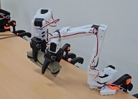
‘Hugging Face’ is a U.S.-based AI startup known as one of the world’s largest platforms for artificial intelligence, offering widely used machine learning libraries such as Transformers and Datasets. More recently, the company has also been actively providing AI resources for robotics applications.
Hugging Face regularly hosts global hackathons that bring together researchers and students from around the world to compete and collaborate on innovative AI-driven solutions.
This year’s ‘LeRobot Worldwide Hackathon’ gathered over 2,500 AI and robotics experts from 45 countries. Participants were challenged to freely propose and implement solutions to real-world problems in industry and everyday life by applying technologies such as VLA (Vision Language Action) models and reinforcement learning to robotic arms.
Through their achievement in the competition, ‘Team ACE’ was recognized for their technical excellence and creativity by both the global robotics community and experts in South Korea.
The team’s performance at the competition drew considerable attention from local media and was actively reported in regional news outlets.
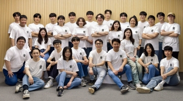
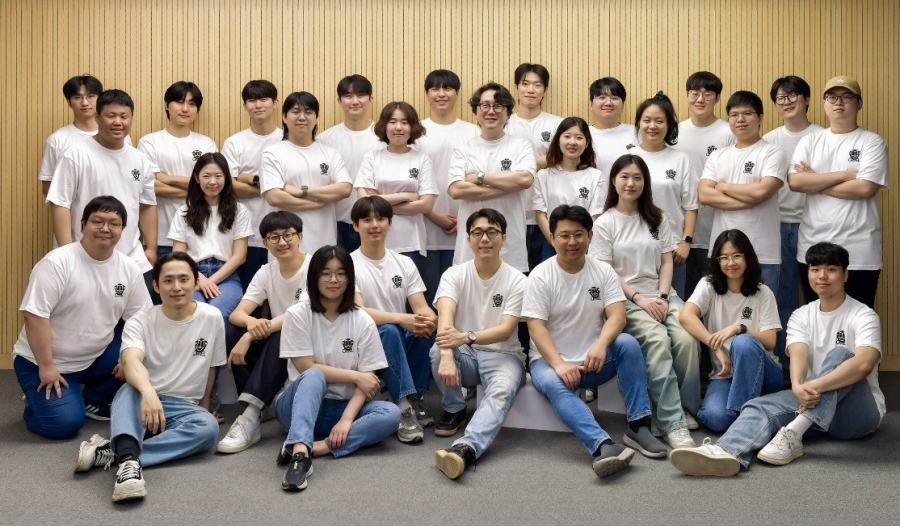
Professor Myoungsoo Jung’s research team is going to reveal their works on next-generation interconnect / semiconductor technologies in IEEE Micro, a leading journal in computer architecture.
IEEE Micro, established in 1981, is a bimonthly publication featuring recent advances in computer architecture and semiconductor technologies. Professor Jung’s team will present a total of five papers in the upcoming May-June issue on “Cache Coherent Interconnects and Resource Disaggregation Technology”.
Among them, three papers focus on applying Compute Express Link (CXL) to storage systems. Especially, the team introduces solutions to improve the performance of CXL-SSD, a concept for which Professor Jung suggested a practical implementation in early 2022. These technologies enable memory expansion through large-capacity SSDs while providing performance comparable to DRAM.
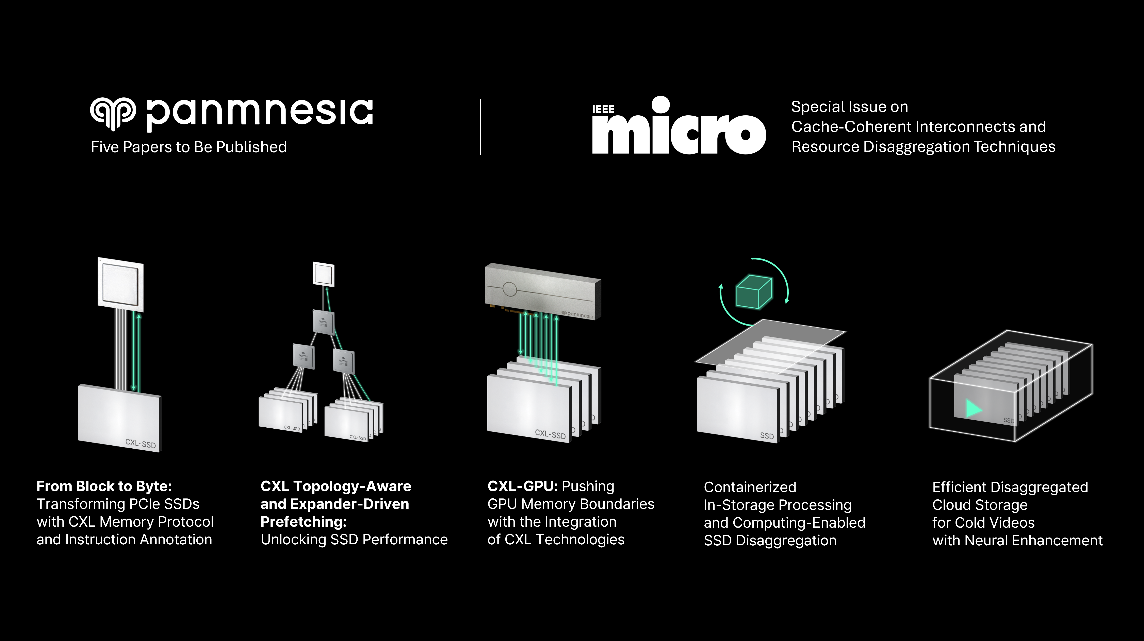
The team also explored storage architectures incorporating In-Storage Processing (ISP), which performs computation directly inside the storage pool. By processing data within storage, this approach reduces data movement and thereby improves efficiency in large-scale applications such as large language models (LLMs).
These papers, conducted in collaboration with the faculty-led startup Panmnesia, will be published through IEEE Micro’s official website and in its regular print issue.
- Early Access Link #1: From Blocks to Byte: Transforming PCIe SSDs with CXL Memory Protocol and Instruction Annotation
- Early Access Link #2: CXL Topology-Aware and Expander-Driven Prefetching: Unlocking SSD Performance
- Early Access Link #3: CXL-GPU: Pushing GPU Memory Boundaries with the Integration of CXL Technologies
- Early Access Link #4: Containerized In-Storage Processing and Computing-Enabled SSD Disaggregation
- Early Access Link #5: Efficient Disaggregated Cloud Storage for Cold Videos with Neural Enhancement
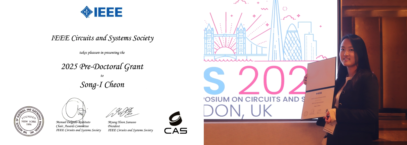
Song-I Cheon, a Ph.D. student in the Department of Electrical and Electronic Engineering under the supervision of Professor Minkyu Je, has been selected as a recipient of the 2025 IEEE Circuits and Systems Society (CASS) Pre-Doctoral Grant.
This prestigious grant is awarded annually to a select number of doctoral students worldwide who have demonstrated outstanding research potential in the field of system semiconductor circuit design. In 2025, only four students globally were selected, with Song-I being one of the recipients.
Song-I has published a total of 19 papers in international journals and conferences, including one paper at ISSCC (as co-first author) and four in IEEE journals (as first or co-first author). Notably, nine of these papers were presented at journals and conferences sponsored by IEEE CASS. Her research contributions in impedance measurement circuit design—particularly in the areas of optimization, high accuracy, and low power consumption—were highly recognized in the selection process.


Alongside large language models, autonomous driving and humanoid robots, AI-driven optimization of industrial manufacturing has emerged as a major application of AI. In 2024, Kim Jeong-hye, a PhD student of Professor Youngchul Sung, interned on LG AI Research’s reinforcement-learning team, where she tackled a range of process-optimization challenges across LG Group’s production facilities.
That team applied optimization majorly based on reinforcement learning to LG Chem’s Daesan plant’s naphtha-cracking facility (NCC), improving production efficiency by 3%, far beyond of 0.1% of initial expectation, and yielding an extra KRW 10 billion in annual profit for that plant alone. Because training reinforcement learning agents via on-line interaction in a production environment is impractical, such optimization typically relies on offline reinforcement learning, which optimizes policies with pre-collected data.
Jeonghye contributed to the development of PARS, a novel offline reinforcement learning algorithm that significantly outperforms existing methods. By enhancing the neural network’s feature resolution with reward scaling with layer normalization, this new approach better differentiates between in-sample and out-of-distribution data, eliminating Q-value divergence, the core issue of off-line reinforcement learning. This advancement promises to accelerate future production-process optimizations as well as many RL applications with difficulty in on-line environment interaction.
This research result will be presented as a Spotlight paper at the International Conference on Machine Learning (ICML) 2025.
Related Yonhap News article: https://www.yna.co.kr/view/AKR20250613153400003
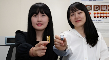
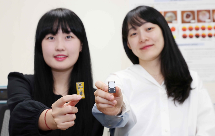

The research team successfully amplified fine vibrations and induced resonance by combining spring-attached 4-stack TENGs. They achieved stable power production of 0.5 mW under conditions of 13 Hz and 0.56 g acceleration. The generated power was then used to operate a CO2 sensor and a Bluetooth Low Energy (BLE) system-on-a-chip (SoC).
Professor Kyeongha Kwon emphasized, “For efficient environmental monitoring, a system that can operate continuously without power limitations is essential.” She explained, “In this research, we implemented a self-powered system that can periodically measure and wirelessly transmit CO2 concentrations based on the energy generated from an inertia-driven TENG.” She added, “This technology can serve as a foundational technology for future self-powered environmental monitoring platforms integrating various sensors.”
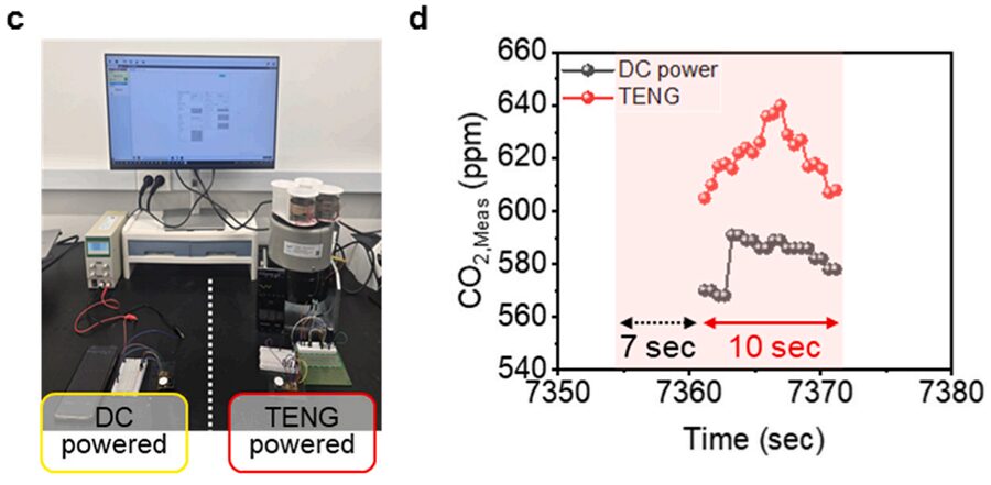
This research was published on June 1st in the internationally renowned academic journal `Nano Energy (IF 16.8)`. Gyurim Jang, a master’s student at KAIST, and Daniel Manaye Tiruneh, a master’s student at Chung-Ang University, are the co-first authors of the paper. *Paper Title: Highly compact inertia-driven triboelectric nanogenerator for self-powered wireless CO2 monitoring via fine-vibration harvesting *DOI: https://doi.org/10.1016/j.nanoen.2025.110872
This research was supported by the Saudi Aramco-KAIST CO2 Management Center.