EE Prof. Kim, SangHyeon’s team, develops display using 3D integration techniques, promising applications on next generation high resolution displays

[ Prof. Kim, SangHyeon, Ju Hyeok Park (P.H.D candidate), Dr. Dae-myeong Geum, Woo Jin Baek (P.H.D candidate), From left]
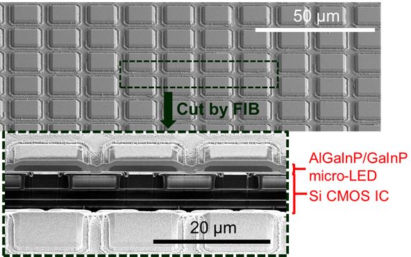
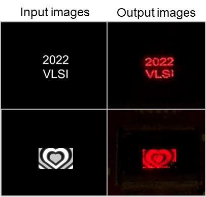
KAIST EE Prof. Kim, SangHyeon’s research team has successfully developed a 1600-PPI MicroLED display by utilizing monolithic 3D integration techniques, as announced.
(*monolithic 3D integration: dubbed the ultimate 3D integration tech, wherein after the lower-layer devices, the upper layer’s thin film is created and stacking proceeds sequentially so as to maximize the upper-lower device alignment)
(* PPI: pixels per inch)
KAIST EE Prof. Kim, SangHyeon Kim’s research team members Ju Hyeok Park and Dr. Dae-myeong Geum led the work as co-first authors, collaborating with Woo Jin Baek from the same research lab and Dr. Johnson Shieh from Jasper Display in Taiwan. Their joint work has been presented at the “semiconductor Olympics”, the 2022 IEEE Symposium on VLSI Technology & Circuits. (Paper: Monolithic 3D sequential integration realizing 1600-PPI red micro-LED display on Si CMOS driver IC)
MicroLED devices using inorganic-based III-V compound semiconductors are gaining attention as core candidates for next-generation ultra-high resolution displays that are growing rapidly in demand. MicroLEDs offer advantages over current OLED and LCD displays widely used in modern TVs and mobile devices with features such as high luminance and contrast ratio, and a longer pixel life.
(*III-V compound semiconductors: Semiconductors comprising of compounds of Group III and Group V elements in the periodic table, offering excellent charge transport and light characteristics)
A monolithic 3D integration of red light-emitting LEDs on a Si CMOS circuit board was applied to solve the issues present in existing device technology. A demonstration of high-resolution display was made successful through continuous semiconductor processes on the wafer. Through this process, the LED semiconductor display layer was designed to reduce the thickness of the active layer for light emission to 1/3 and greatly reduce the challenges of the etching process required for pixel formation. In addition, to prevent performance degradation of the lower display driving circuit, the research team was able to maintain the performance of the lower Driver IC even after the integration of the upper layer by using ultra-low temperature processes such as wafer bonding that integrates the upper III-V layer below 350 C.
By successfully implementing state-of-the-art resolution of 1600-PPI MicroLED display using a monolithic 3D integration of red LEDs, this result is expected pave way for the next-generation ultra-high resolution displays.
Image 1.

Image 2.
