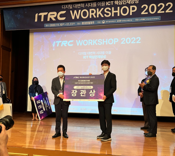
Professor Youngsoo Shin receives the October Scienc and Technology Award, Optimizing Semiconductor Process with AI

[Professor Youngsoo Shin receives the October Scienc and Technology Award, Optimizing Semiconductor Process with AI]
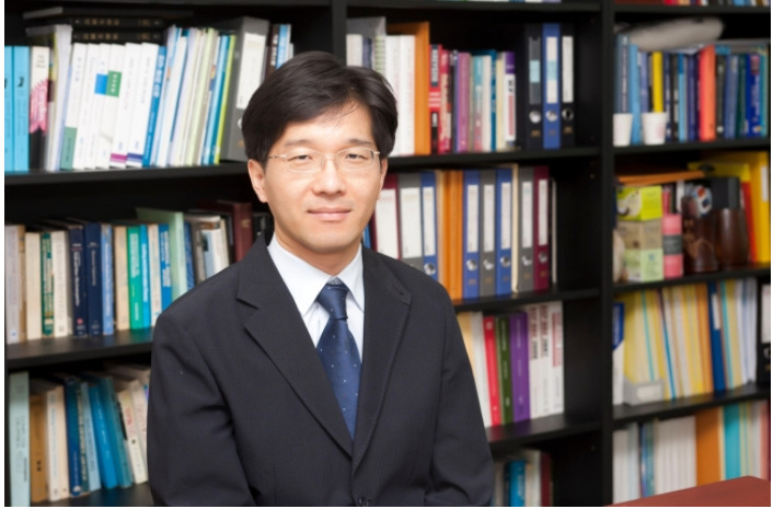
 

651f50dab0926

<Professor Youngsoo Shin>


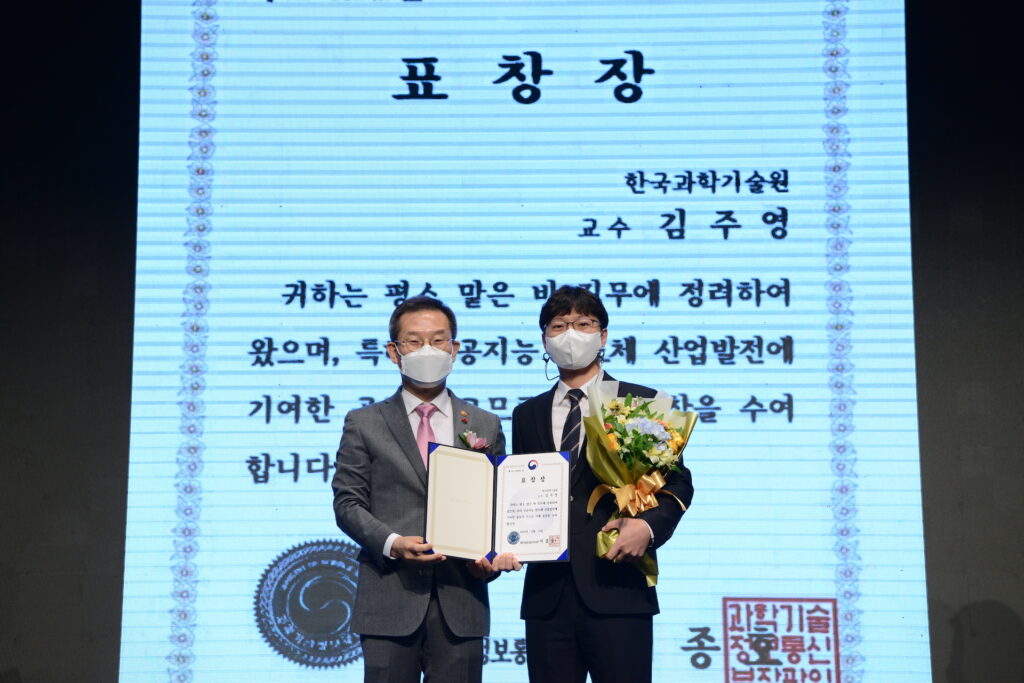
The Ministry of Science and ICT and the Korea Research Foundation announced on the 4th that Professor Shin Youngsoo from the School of Electrical Engineering at KAIST was selected as the winner of the ‘Science and Technology Award’ for October. 

Professor Shin was recognized for his contribution in developing a semiconductor lithography optimization technology that is 10 times faster and has a higher resolution than existing methods using machine learning.


Lithography is a process in which light is shone on a mask engraved with patterns to create devices on a wafer.

It is a critical process that determines the yield of semiconductors. In order to create polygons on the wafer, complex patterns must be drawn on the mask.

This process,  known as OPC (Optical Proximity Correction), involves repeatedly adjusting the mask shape and simulating the image on the wafer, taking a significant amount of time.


Professor Shin trained artificial intelligence (AI) on sets of mask shapes and the resulting wafer images to develop a faster and higher-resolution OPC optimization technique.

 Additionally, Professor Shin developed a method to create a layout pattern (semiconductor blueprint) similar in structure to existing patterns but not previously existing, using generative AI.


It was also confirmed that applying the newly created layout patterns and the existing sample patterns to the optimization improves the accuracy of the machine learning model.

The research results were published in the 2021 international academic journal IEEE TSM, and it also received the journal’s ‘Best Paper Award,’ which is selected once a year.


Professor Shin commented, “This study is unique in that it applies machine learning and artificial intelligence differently from existing semiconductor lithography research,” and added, “I hope it can contribute to resolving the issues of licensing costs and stagnation in technological development caused by the monopoly of a small number of companies worldwide.”


*Reference : 10월 과기인상에 신영수 교수…AI로 반도체 공정 최적화 (naver.com)

EE Professor Kim Joo-Young Developed A ChatGPT Core AI Semiconductor with A 2.4-fold Improvement in Price efficiency

EE Professor Kim Joo-Young Developed A ChatGPT Core AI Semiconductor with A 2.4-fold Improvement in Price efficiency


The ChatGPT released by OpenAI has captured global attention, and everyone is closely observing the changes this technology will bring out.

This technology is based on large language models (LLM), which represent an unprecedented scale of artificial intelligence (AI) models compared to conventional AI.

However, the operation of these models requires a significant number of high-performance GPUs, leading to astronomical computing costs.  


KAIST (President: Lee Kwang-Hyung) announced that research team led by EE Professor Kim Joo-Young Kim has successfully developed an AI semiconductor that efficiently accelerates the inference operations of large language models, which play a crucial role in ChatGPT. 

The developed AI semiconductor, named the ‘Latency Processing Unit (LPU),’ efficiently accelerates the inference operations of large language models. It incorporates a high-speed computing engine capable of maximizing memory bandwidth utilization and performing all necessary inference computations rapidly.

Additionally, it comes equipped built-in networking capabilities, making it easily expandable with multiple accelerators. This LPU-based acceleration appliance server achieved up to a 50% higher performance and approximately 2.4 times better performance-to-price ratio compared to a supercomputer based on the industry-leading high-performance GPU, NVIDIA A100.


This advancement holds the potential to replace high-performance GPUs in data centers that are experiencing a rapid surge in demand for generative AI services. This research was conducted by Professor HyperExcel Co., founded by Professor Kim Joo-Young and achieved the remarkable accomplishment of receiving the “Engineering Best Presentation Award” at the International Design Automation Conference (DAC 2023) held in San Francisco on July 12th (U.S. time).

DAC is a prestigious international conference in the field of semiconductor design, particularly showcasing global semiconductor design technologies related to Electronic Design Automation (EDA) and Semiconductor Intellectual Property (IP).

DAC attracts participation from renowned semiconductor design companies such as Intel, NVIDIA, AMD, Google, Microsoft, Samsung, TSMC, as well as top universities including Harvard, MIT, and Stanford.


Among the world’s notable semiconductor technologies, Professor Kim’s team stands out as the sole recipient of an award for AI semiconductor technology tailored for large language models.

This award acknowledges their AI semiconductor solution as a groundbreaking means to drastically reduce the substantial costs associated with inference operations for large language models on the global stage.


Professor Kim stated, “With the new processor ‘LPU’ for future large AI computations, I intend to pioneer the global market and take a lead over big tech companies in terms of technological prowess.”

(Note: The provided translation is an elaboration and summary of the original text for clarity and readability.)


영문

[Related News]
Chosun Ilbo : 챗GPT 가성비 2.4배 높이는 반도체 나왔다 – 조선비즈 (chosun.com) 
DongA Science : 챗GPT 효율 높일 ‘AI 반도체’ 개발…국제학회서 ‘최고 발표상’ : 동아사이언스 (dongascience.com) 
 

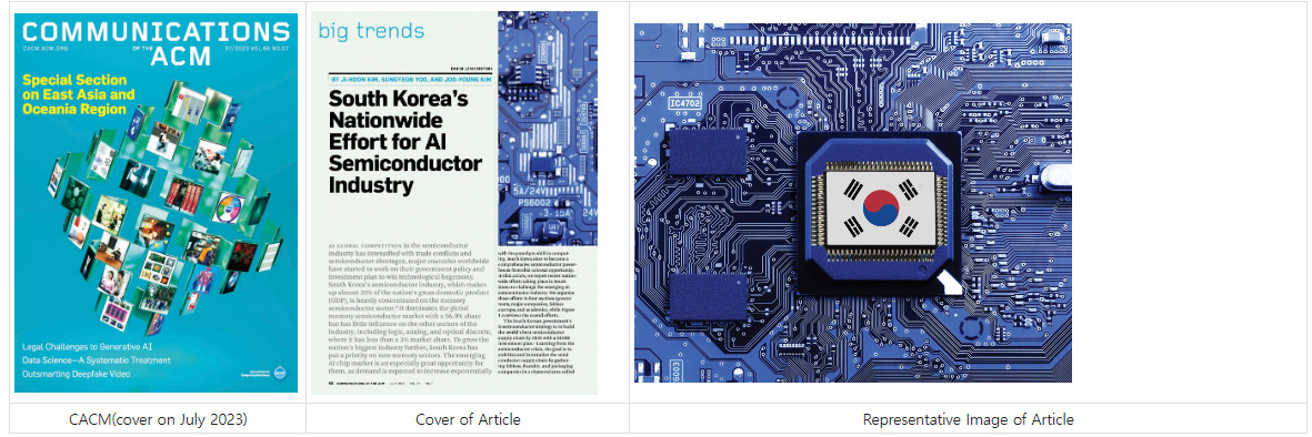
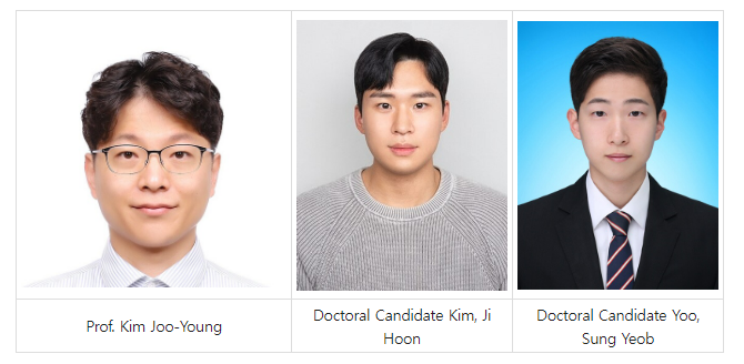
Professor Joo-Young Kim’s Research Team Published Article in CACM Magazine: “South Korea’s Nationwide Effort for AI Semiconductor Industry”

Professor Joo-Young Kim’s Research Team Published Article in CACM Magazine: “South Korea’s Nationwide Effort for AI Semiconductor Industry”


Recently, the research team led by Professor Joo-Young Kim published an article titled “South Korea’s Nationwide Effort for AI Semiconductor Industry” in CACM (Communications of the ACM), one of the leading monthly academic journals in the field of computer science.


64bf2a8b126e4


In this article, Professor Joo-Young Kim’s research team provides an in-depth analysis of the national efforts for the AI semiconductor industry currently underway in South Korea. They thoroughly examine the multifaceted endeavors carried out by the government, industry, and academia.
 
The article sheds light on the government’s investment plans to establish a world-class semiconductor supply chain, the ambitious AI semiconductor projects of major companies such as Samsung Electronics and SK hynix, and the rise of startups like Furiosa, Rebellions, SAPEON, HyperAccel, OpenEdge, Mobilint, DeepX, and Telechips, which are developing AI accelerators for specific application areas.
 
Additionally, the article introduces the Semiconductor Systems Department at KAIST, as well as AISS and PIM research centers, and showcases various programs provided by IDEC for research support in chip design.
 
This article provides insight into South Korea’s development direction and achievements in the field of AI semiconductors, which combine strategic technological advancements at the national level and active participation from businesses. Its international dissemination holds significant meaning.
 
For those interested in exploring insights into the future of the AI semiconductor industry and upcoming technologies, we recommend reading this article.
Link: https://dl.acm.org/doi/10.1145/3587264
 
 
연구팀영문


EE Professor Minkyu Je is awarded the Haedong Semiconductor Engineering Award.

EE Professor Minkyu Je is awarded the Haedong Semiconductor Engineering Award.


Professor Minkyu Je of our department won the “Haedong Semiconductor Engineering Award” at the 2022 regular meeting of the Semiconductor Engineering Society held at the Seoul aT Center on December 7th.

The Haedong Science and Culture Foundation has made a lot of effort and dedication to discovering and motivating talent for technological development and industry in Korea.

In particular, in 2021, the “Haedong Semiconductor Engineering Award” was established for the semiconductor industry and technology to provide a cornerstone for discovering semiconductor talent.

This year’s 2nd “Haedong Semiconductor Engineering Award” is more meaningful because it is given now that the importance of the semiconductor field is being highlighted more than ever in the world


Photo Minkyu Je long

[Prof. Minkyu Je]


Professor Minkyu Je has conducted leading research in the field of biomedical and sensor interface integrated circuits/microsystems since the early 2000s while working at the IME Research Center under A*STAR in Singapore. He was awarded because it played an important role in leading the level of domestic research in this field to the world level by continuing the highest level of research. 

Since he has played an important role in leading the level of domestic research in this field to the world level by continuing the highest level of research, he was awarded. He is recognized internationally as a major researcher who has greatly contributed to the pioneering and development of the field, and is playing a role as a leading researcher in this field in Korea.

 In recognition of excellent research achievements in the field of circuits and systems for next-generation medical devices and neuronal interfaces, he was selected as a Distinguished Lecturer by the IEEE Circuits and Systems Society (CASS) in 2020, and he presented a total of 110 SCI journal papers and 252 international conference papers.

 In particular, a total of 76 papers were published in various IEEE excellent journals related to the field, and a total of 25 papers were presented at the highest level international conferences, IEEE ISSCC, IEEE SOVC, and IEEE CICC. 

In addition, through research in this field, a total of 24 foreign patents and a total of 26 domestic patents were registered, and a total of 30 patents are pending domestic/overseas applications. 

Through active cooperation with start-ups and SMEs as well as large companies in related fields, he has significantly contributed to securing technological competitiveness in the bio/medical device and IoT sensor fields, creating and revitalizing the industrial ecosystem, and securing future growth engines targeting emerging markets. 


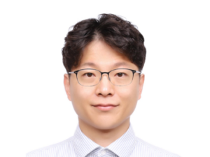
EE professor Joo-Young Kim receives the Science and ICT Minister’s Award at the 2022 Future AI Semiconductor Technology Conference

EE professor Joo-Young Kim receives the Science and ICT Minister’s Award

 
Professor Joo-Young Kim has won the Science and ICT Minister’s award on December 12th at the 2022 Future AI Semiconductor Technology Conference, held at the Gyeonggi Center for Creative Economy & Innovation, Pangyo. 
 
Professor Kim was recognized for his contribution within the artificial intelligence semiconductor industry.
Professor Kim’s works within the field include the national research and development of AI processors and PIM semiconductor technologies, as well as fostering future semiconductor engineers and contributing to fabless ecosystems.
 
Recently, he is actively researching AI semiconductors and hybrid memory-logic PIM semiconductors, for the application in large AI models.
 
jyKim 1 e1663644687523 360x270 1
[Prof. Joo-Young Kim ]
 
LGW 5192
[Awards ceremony]


MS course Wonhoon Park (Prof. Hoi-Jun Yoo), won the Distinguished Design Award at ’22 IEEE A-SSCC

캡처

[Prof. Hoi-Jun Yoo,  Wonhoon Park ]
 
EE MS student  Wonhoon Park (Advised by Hoi-Jun Yoo), won the Distinguished Design Award at the 2022 IEEE Asian Solid-State Circuits Conference (A-SSCC) Student Design Contest.
The conference was held in Taipei, Taiwan from November 6th to 9th.
 
A-SSCC is an international conference held annually by IEEE. M.S. student Wonhoon Park has published a paper titled “An Efficient Unsupervised Learning-based Monocular Depth Estimation Processor with Partial-Switchable Systolic Array Architecture in Edge Devices” and was selected as a winner for its excellence.
 
Details are as follows. 
 
-Conference: 2022 IEEE Asian Solid-State Circuits Conference (A-SSCC)
-Location: Taipei, Taiwan
-Date: November 6-9, 2022
-Award: Student Distinguished Design Award
-Authors: Wonhoon Park, Dongseok Im, Hankyul Kwon, and Hoi-Jun Yoo (Advisory Professor)
-Paper Title: An Efficient Unsupervised Learning-based Monocular Depth Estimation Processor with Partial-Switchable Systolic Array Architecture in Edge Devices

Professor Joo-Young Kim’s Center (Artificial Intelligence Semiconductor System Research Center) won the Minister of Science and Technology Information and Communication Award

dataURItoBlob 1

[Prof. Joo-Young Kim ]
 
On November 10, the Artificial Intelligence Semiconductor System Research Center (AISS), led by Professor Joo-Young Kim of KAIST, was awarded the Minister of Science, Technology and Information Technology Award in recognition of its outstanding talent cultivation performance.
 
AISS, headed by Professor Joo-Young Kim, has been carrying out the university ICT research center fostering support project of the Ministry of Science and ICT since 2020, dedicating efforts to nurturing talented people from various angles.
 
Particularly in 2021, 96 student researchers were continuously educated through various themes and programs such as internships, technology transfer, entrepreneurship education, and creative initiatives. It has become a model for other centers by recording remarkable achievements such as employment.
 
AISS is currently carrying out active research activities under the project responsibility of Professor Joo-Young Kim, KAIST Research Director, Hoe-Jun Yoo, Yi-Seop Kim, In-Cheol Park, Seung-Tak Ryu, Hyun-Sik Kim, Yonsei University Han-Jun Kim, Jin-Ho Song, Ji-Hoon Kim, Seong-Min Park of Ewha Womans University, and Kyu-Ho Lee of UNIST. In addition, there has been a 10% increase from 2021 with 110 masters and doctoral-level students participating in taking a strong step towards becoming a Korean hub in the field of artificial intelligence semiconductors.
 
Professor Joo-Young Kim, the research director who won the award, said, “We will continue to strengthen the link with leading universities and companies in Korea based on the university’s ICT and intelligent semiconductor technology capabilities to foster system semiconductor manpower essential for Korea to become a true semiconductor technology powerhouse.”
 
사진 dataURItoBlob


KAIST EE Professor Hyun-Sik Kim’s team, Prime Minister’s Award at the 23rd Korea Semiconductor Design Challenge

캡처

[Prof. Hyun-Sik Kim,  PhD candidate Gyuwan Lim, PhD candidate  Gyeong-Gu Kang, from left]


EE professor Hyun-Sik Kim’s team of Ph.D. students received the Prime Minister’s Award at the 23rd Korea Semiconductor Design Challenge.


The 23rd Korea Semiconductor Design Challenge is held to cultivate design skills and discover creative ideas of students within the field of semiconductor design, jointly organized by the Korean Ministry of Trade, Industry and Energy, and the Korea Semiconductor Industry Association (KSIA).


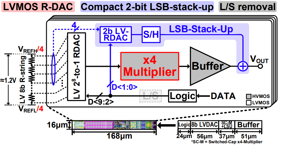
The winners, Gyuwan Lim and Gyeong-Gu Kang, have been selected for the achievement of high resolution and high uniformity with their mobile device Display Driver IC (DDI) design while maintaining an ultra-small chip area.


The DDI chip is a key component of a display system, that converts digital display data into analog signals (digital-to-analog conversion, DAC) and writes them to the display panel. The KAIST team solved the problem of uniformity and increasing chip surface that comes with higher resolution DDI chips.


The award-winning DDI chip design consists of a low-voltage MOSFET with a voltage amplifier instead of the conventional high-voltage MOSFET. This technology dramatically reduces the channel area, further reduced through a novel LSU technology that generates a 10-bit output voltage from an 8-bit input voltage.


The team was able to achieve high uniformity through designing a robust amplifier and chip operation against variations of the CMOS fabrication process. The novel DDI chip design is expected to significantly reduce cost while increasing the quality of mobile device displays through the reduced chip area, while achieving high resolution and high uniformity at the same time.


The results of this study were also presented at ISSCC 2022, a highly reputable international conference in the field of integrated circuits.


1 제안하는 Display Driver 구조 및 사용 기술


Design of Processing-in-Memory with Triple Computational Path and Sparsity Handling for Energy-Efficient DNN Training

Title : Design of Processing-in-Memory with Triple Computational Path and Sparsity Handling for Energy-Efficient DNN Training

Authors : Wontak Han, Jaehoon Heo, Junsoo Kim, Sukbin Lim, Joo-Young Kim

Publications : IEEE Journal on Emerging and Selected Topics in Circuits and Systems (JETCAS), 2022

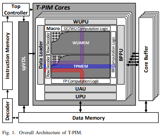
As machine learning (ML) and artificial intelligence (AI) have become mainstream technologies, many accelerators have been proposed to cope with their computation kernels. However, they access the external memory frequently due to the large size of deep neural network model, suffering from the von Neumann bottleneck. Moreover, as privacy issue is becoming more critical, on-device training is emerging as its solution. However, on-device training is challenging because it should perform the training under a limited power budget, which requires a lot more computations and memory accesses than the inference. In this paper, we present an energy-efficient processing-inmemory (PIM) architecture supporting end-to-end on-device training named T-PIM. Its macro design includes an 8T-SRAM cell-based PIM block to compute in-memory AND operation and three computational datapaths for end-to-end training. Each of three computational paths integrates arithmetic units for forward propagation, backward propagation, and gradient calculation and weight update, respectively, allowing the weight data stored in the memory stationary. T-PIM also supports variable bit precision to cover various ML scenarios. It can use fully variable input bit precision and 2-bit, 4-bit, 8-bit, and 16-bit weight bit precision for the forward propagation and the same input bit precision and 16-bit weight bit precision for the backward propagation. In addition, T-PIM implements sparsity handling schemes that skip the computation for input data and turn off the arithmetic units for weight data to reduce both unnecessary computations and leakage power. Finally, we fabricate the T-PIM chip on a 5.04mm2 die in a 28-nm CMOS logic process. It operates at 50–280MHz with the supply voltage of 0.75–1.05V, dissipating 5.25–51.23mW power in inference and 6.10-37.75mW in training. As a result, it achieves 17.90–161.08TOPS/W energy efficiency for the inference of 1-bit activation and 2-bit weight data, and 0.84–7.59TOPS/W for the training of 8-bit activation/error and 16-bit weight data. In conclusion, T-PIM is the first PIM chip that supports end-to-end training, demonstrating 2.02 times performance improvement over the latest PIM that partially supports training.

2

T-PIM: A 2.21-to-161.08TOPS/W Processing-In-Memory Accelerator for End-to-End On-Device Training

Title : T-PIM: A 2.21-to-161.08TOPS/W Processing-In-Memory Accelerator for End-to-End On-Device Training

Authors : Jaehoon Heo, Junsoo Kim, Wontak Han, Sukbin Lim, Joo-Young Kim

Publications : IEEE Custom Integrated Circuits Conference (CICC) 2022

As the number of edge devices grows to tens of billions, the importance of intelligent computing has been shifted from cloud datacenters to edge devices. On-device training, which enables the personalization of a machine learning (ML) model for each user, is crucial in the success of edge intelligence. However, battery-powered edge devices cannot afford huge computations and memory accesses involved in the training. Processing-in-Memory (PIM) is a promising technology to overcome the memory bandwidth and energy problem by combining processing logic into the memory. Many PIM chips [1-5] have accelerated ML inference using analog or digital-based logic with sparsity handling. Two-way transpose PIM [6] supports backpropagation, but it lacks gradient calculation and weight update, required for end-to-end ML training.

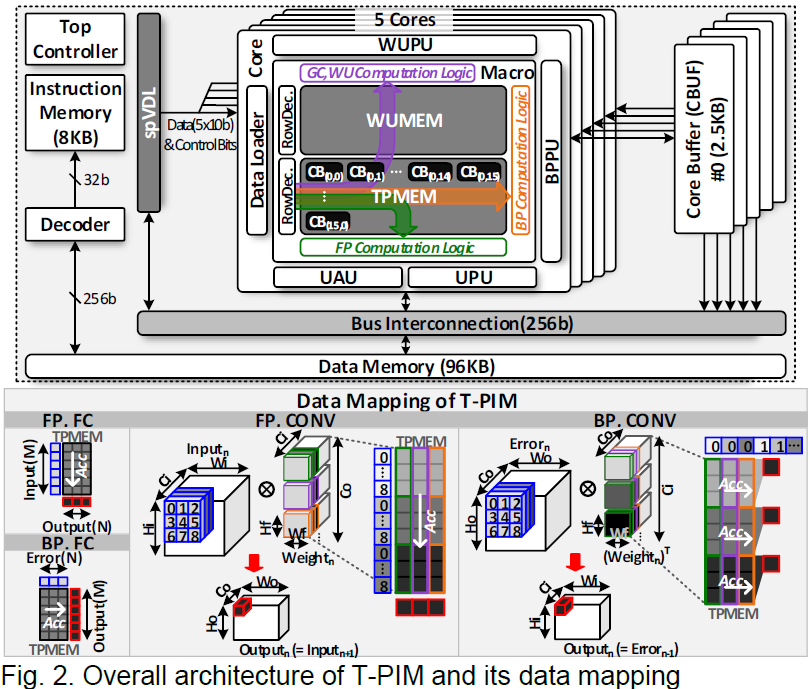
This paper presents T-PIM, the first PIM accelerator that can perform end-to-end on-device training with sparsity handling and support low-latency ML inference. T-PIM makes the four key contributions: 1) T-PIM can run the complete four computational stages of ML training on a chip (Fig. 1). 2) T-PIM allows various data mapping strategies for two major computational layers, i.e., fully-connected (FC) and convolutional (CONV), as well as two computational directions, i.e., forward and backward. 3) T-PIM supports fully variable bit-width for input data and power-of-two bit-width for weight data using serial and configurable arithmetic units. 4) T-PIM accelerates and saves energy consumption in ML training by exploiting fine-grained sparsity in all data types (act., error, and weight).


1