






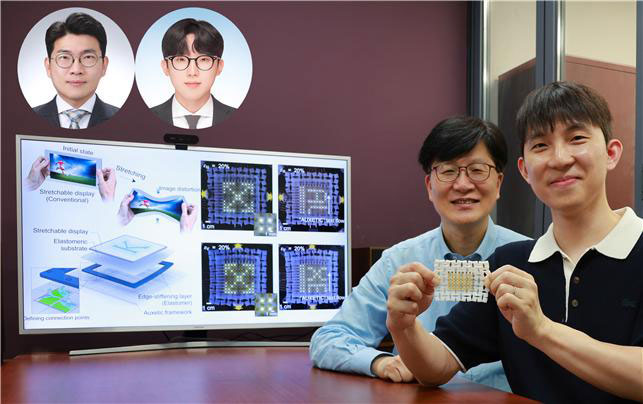
Beyond bendable and foldable displays, the era of stretchable displays, whose screens can expand freely like rubber, is now emerging. KAIST researchers have developed a core technology that allows text, images, and other on-screen information to retain their original shape even when the screen is stretched by up to 15%. The achievement is expected to help solve the problem of image distortion and accelerate the commercialization of next-generation high-quality stretchable displays.
The research team led by Professor Seunghyup Yoo of the School of Electrical Engineering, in collaboration with Professor Hanul Moon’s team at Dong-A, has successfully implemented an auxetic-based stretchable display platform. Auxetic structures expand in both width and length when pulled, allowing the display to stretch uniformly at the same ratio in all directions without distorting the image on the screen.
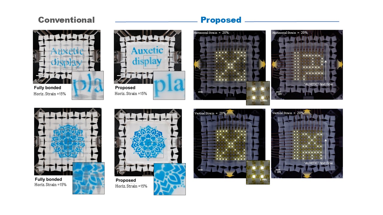
Conventional stretchable displays are generally made by forming light-emitting devices on a stretchable substrate, which serves as the base layer of the display. However, when such a substrate is stretched in one direction, it tends to shrink in the opposite direction, causing letters and images on the screen to become flattened or distorted. Auxetic structures have been used to address this problem, but most previous approaches were limited to maintaining the overall horizontal-to-vertical ratio of the screen, while the letters and images within the screen still remained vulnerable to distortion.
Instead of bonding the auxetic structure and the stretchable substrate across the entire surface, as in conventional methods, the research team proposed a new design approach that uses computational analysis to selectively connect only the necessary points that ensure isotropic expansion throughout the substrate.
In the conventional approach, the twisting deformation that occurs as the auxetic structure stretches is directly transferred to the substrate, distorting the image inside the screen. In contrast, the platform developed by the research team was designed so that each region moves evenly outward from its original position. This allows not only the entire screen but also small areas such as letters and images to expand together while maintaining their original shapes.

The research team verified the platform’s performance by repeatedly stretching a substrate patterned with letters and images in both the horizontal and vertical directions. In the conventional method, the patterns underwent local deformation, whereas in the new platform, the shapes of the letters and images remained intact. This demonstrates that not only the whole screen but also fine images on-screen can expand uniformly without distortion.
The team also integrated an LED array, a structure in which multiple LEDs are arranged at regular intervals, onto the platform to verify its performance as a working stretchable display. Even when stretched by up to 15% in both the horizontal and vertical directions, stable electrical operation and the screen brightness were maintained. After repeated stretching to 15%, the decrease in brightness remained below 2%, confirming the platform’s potential for practical display applications.
This technology is expected to serve as a core platform for next-generation electronics with freely changeable shapes, including wearable electronic devices, electronic skin, or e-skin, which refers to electronic devices that stretch like skin while sensing and displaying information, medical biosensors, soft robots, and curved displays for automobiles and aircraft.
Professor Seunghyup Yoo of KAIST said, “For stretchable displays to be used as actual information display devices, they must not only stretch well, but also preserve on-screen information accurately during stretching,” adding, “This platform enables uniform expansion from small areas of the screen to the entire display, and will serve as a key foundational technology for accelerating the commercialization of high-quality stretchable displays.”
This study was led by KAIST Dr. Su-Bon Kim and Dr. Junho Kim as co-first authors, with Professor Hanul Moon of Dong-A University and Professor Seunghyup Yoo of KAIST as co-corresponding authors. The research was published in the international journal Nature Communications on June 10.
- Paper title: Hybrid auxetic metamaterial platforms enabling multiscale isotropic expansion for distortion-free stretchable displays
- DOI: 10.1038/s41467-026-74141-6
- Demonstration Video: https://bit.ly/4gSRf8W
This research was supported by the National Research Foundation of Korea (NRF) Mid-Career Researcher Program, the Future Display Strategic Research Laboratory Program, the Korea Planning & Evaluation Institute of Industrial Technology (KEIT), and theKorea Institute for Advancement of Technology (KIAT) HRD Program.

Artificial intelligence (AI) is rapidly evolving beyond simply answering questions into the era of “AI agents,” which can perform complex tasks by autonomously carrying out multi-step reasoning and using external tools. However, the extent to which these advances require additional resources and power has not been properly quantified until now.
A research team led by KAIST School of Electrical Engineering Chair Professor Minsoo Rhu has announced the first quantitative analysis of AI agents’ computational cost, response latency, energy consumption, and their broader impact on data center power demand. The findings were presented at IEEE HPCA 2026, one of the most prestigious conferences in the field of computer architecture, drawing significant attention from the academic community.
The research team focused on the fact that AI agents do not merely increase computational workload, but also impose a fundamentally new burden on data center infrastructure. Unlike conventional “chain-of-thought” reasoning, which proceeds step by step in a manner similar to human reasoning, AI agents operate by repeatedly invoking large language models (LLMs) throughout the task execution process.
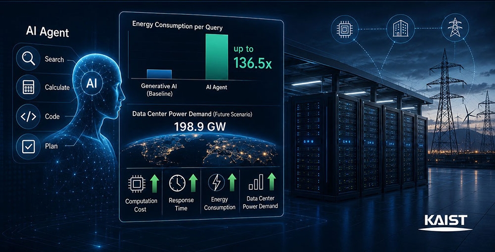
The analysis found that AI agents triggered, on average, 9.2 times more LLM invocations than conventional approaches, while processing latency increased by as much as 153.7 times. In addition, during tool-use phases, GPUs inevitably remained idle, with idle time accounting for up to 54.5% of the total execution time. This means that as tasks become more complex, the inefficiency of underutilizing expensive GPUs becomes increasingly severe.
When extrapolated to the scale of data centers, the gap in power consumption becomes even more pronounced. An AI agent using a 70-billion-parameter LLM, comparable to the scale of today’s commercial AI services, consumed an average of 348.41 Wh to process a single query. This is approximately 136.6 times higher than the 2.55 Wh consumed by a conventional one-shot question-answering approach.
The resulting power burden on data centers could grow exponentially. If at least 71.4 million daily active ChatGPT users were to shift from conventional question-answering to AI agents, the required power would jump from 7.6 MW to 1 GW. If approximately 13.7 billion Google searches per day were to be handled by AI agents in the future, the required power would amount to 198.9 GW per day. This is a massive figure equivalent to nearly half of the average total power load of the United States, which stands at 476.9 GW.
“The significance of this study lies in showing that improving AI agent capabilities does not merely require more computation, but also creates a new class of burden across data center infrastructure,” the research team said. “Future research on AI agents must consider not only how to build smarter agents, but also how to operate them efficiently within limited infrastructure and power budgets.”
Kiyoung Choi, former professor at Seoul National University’s Department of Electrical and Computer Engineering and former Minister of Science and ICT, noted that in addition to the challenges surrounding AI data centers, semiconductor shortages, and material constraints, power supply is also a highly difficult issue. He emphasized the significance of this paper in sounding an alarm that endlessly expanding data center scale and cost in response to AI agents’ demands may not be sustainable.
The study was conducted by Master’s student Byungjun Shin, MS-PhD integrated student Jinha Jung, and PhD student Jiin Kim.
※ Paper title: The Cost of Dynamic Reasoning: Demystifying AI Agents and Test-Time Scaling from an AI Infrastructure Perspective
※ GitHub technical open source: https://github.com/VIA-Research/AgentBench
This work was supported by the SW Computing Industry Core Technology Development Program, including the SW Starlab Program, funded by the Ministry of Science and ICT and the Institute of Information & Communications Technology Planning & Evaluation, as well as by the Samsung Science & Technology Foundation.
Major Media Coverage
- 이데일리: “AI 에이전트, 질문 한 번에 전력 136배 더 쓴다”…KAIST, 세계 첫 정량 분석 (2026.7.5)
- 헤럴드경제: “챗GPT보다 전력소모 136.5배↑”…KAIST, AI 에이전트 ‘숨은 전력 비용’ 첫 규명 (2026.7.5)
- 파이낸셜뉴스: 똑똑하다는 ‘AI 비서’, 알고 보니 전기먹는 하마? 전력 소모량 136배 많아 (2026.7.5)
- 디지털데일리: 에이전트AI, 생성AI보다 전력 소모 ‘136.5배’↑…”에너지 인프라 중요성 부각” (2026.7.5)
- 한국일보: AI 에이전트는 전기 먹는 하마? “생성형 AI보다 136배 더 써” (2026.7.5)
- 한겨레: ‘답변’ 아닌 ‘과제’ 수행하는 AI, 에너지 소비 136.6배 많아 (2026.7.5)


Future vehicles will control not only their motors but also the flow of air around them. Researchers at KAIST have developed an active aerodynamic technology that continuously adjusts airflow according to driving conditions, improving both the performance and safety of high-performance electric vehicles.
The research team led by Professor Hyunchul Shim in the School of Electrical Engineering, with support from Hyundai Motor Company, has developed a Multi-Surface Active Aerodynamic System capable of integrated control of multiple aerodynamic devices installed at the front and rear of a vehicle. The proposed technology was successfully implemented and validated on a full-scale vehicle under real circuit driving conditions.
The study, led by Sungwon Nah, a Ph.D. candidate and first author, received the First Prize Best Student Paper Award at the 2026 IEEE Intelligent Vehicles Symposium (IV 2026), held in Detroit, Michigan, USA, in June 2026.
This award represents the highest honor presented to the most outstanding student paper at the conference. The research was first selected for an Oral Presentation, a distinction awarded to only approximately 8.5% of accepted papers, and subsequently won the First Prize Best Student Paper Award following the final evaluation of the oral presentations, recognizing both its originality and technical excellence.
The IEEE Intelligent Vehicles Symposium (IV), organized by the IEEE Intelligent Transportation Systems Society (ITSS), is one of the world’s premier international conferences in the field of intelligent vehicles. It brings together leading researchers from universities, research institutes, and the automotive industry to present the latest advances in autonomous driving, vehicle control, artificial intelligence (AI), and future mobility technologies.
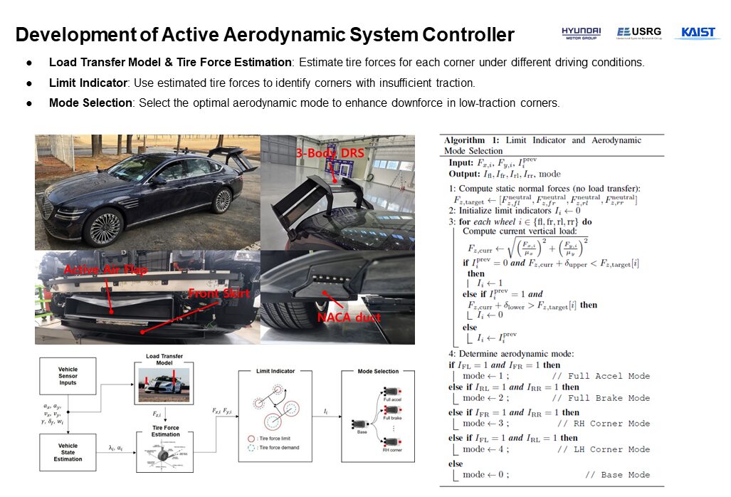
To achieve integrated control of four active aerodynamic devices mounted on the front and rear of the vehicle, the research team first established an aerodynamic model based on wind tunnel experiments that accurately captured the aerodynamic characteristics of each device.
Building on this model, the researchers developed a real-time control framework that continuously analyzes driving conditions, including vehicle speed and steering state, to determine the optimal aerodynamic mode. The proposed framework was validated through both high-fidelity vehicle simulations and full-scale vehicle experiments.
Unlike many previous studies that have been limited to simulation-based validation, the team conducted full-scale vehicle testing at the Korea International Circuit (KIC), an FIA Grade 1 circuit certified to host Formula One races, thereby demonstrating the practicality and effectiveness of the proposed technology under real driving conditions.
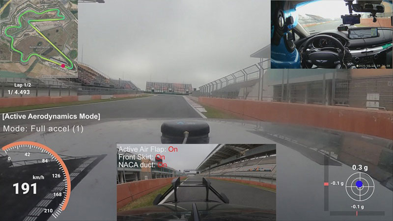
Experimental results showed that the proposed active aerodynamic system effectively improved lap time, braking performance, cornering performance, and overall vehicle stability in high-performance electric vehicles. Furthermore, the consistent performance improvements observed in both simulation and real-world experiments demonstrate the technology’s strong potential for future applications not only in high-performance electric vehicles but also in autonomous vehicles and Software-Defined Vehicles (SDVs), whose capabilities can be continuously enhanced through software updates.
The first author, Sungwon Nah, also served as the team leader of KAIST EURECAR in the Indy Autonomous Challenge (IAC), an international autonomous racing competition in which Professor Shim’s laboratory has participated since 2021. Under his leadership, the team successfully achieved autonomous driving at speeds of up to 290 km/h, accumulating world-class expertise in high-speed autonomous vehicle control that directly contributed to this research.
Professor Hyunchul Shim said, “This recognition at one of the world’s most prestigious conferences on intelligent vehicles is particularly meaningful because it is built upon the practical experience our laboratory has accumulated through high-speed autonomous racing competitions such as the Indy Autonomous Challenge. We expect this research to contribute not only to improving the performance of high-performance electric vehicles but also to enhancing the safety and driving capabilities of future intelligent vehicles.“
The paper was led by Sungwon Nah (Ph.D. candidate) as first author, with Seungjin Yang, Youngjun Hwang, and Jungha Wang (M.S. students) as co-authors. Researchers Janghan Choi, JungSoo Lee, and JungKi Son from Hyundai Motor Company also participated as collaborators.
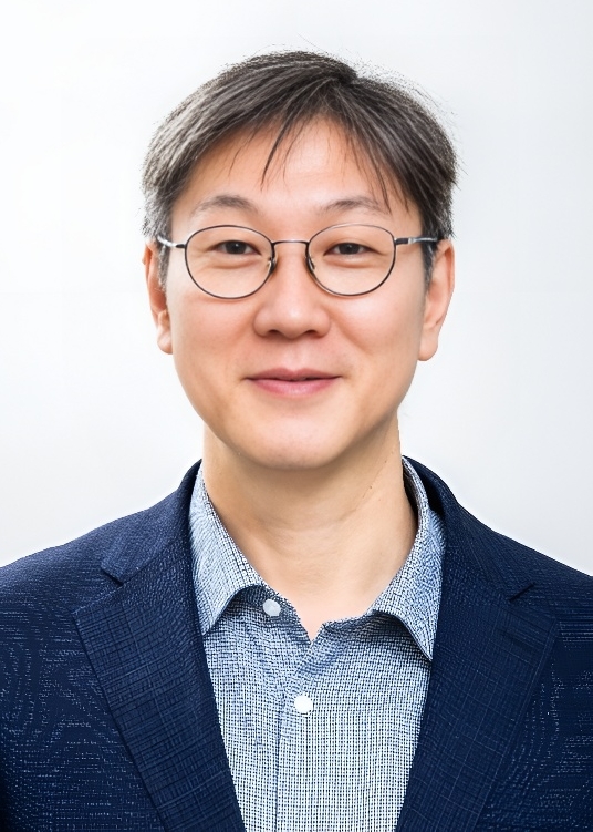
We are pleased to announce that Professor Kihwan Kim, Director of the IBS Center for Trapped Ion Quantum Science at the Institute for Basic Science (IBS), has joined the KAIST School of Electrical Engineering as an Adjunct Professor, effective June 26, 2026.
Professor Kim is a leading scholar recognized for his pioneering contributions to trapped-ion quantum computing and quantum simulation. His research focuses on developing scalable quantum computing platforms and programmable quantum simulators by integrating precision optical and electronic control technologies with quantum hardware system design.
His main research interests span trapped-ion quantum computing hardware, laser- and microwave-based qubit control, multi-qubit quantum gates, two-dimensional ion crystals, quantum simulation, and quantum systems for modeling quantum chemistry and materials.
Professor Kim has published numerous landmark studies in world-renowned journals, including the demonstration of single-ion qubit coherence times exceeding one hour (Nature Communications, 2021), the realization of programmable Ising models using all-to-all entangling gates (Nature, 2019; PRL, 2025), quantum simulation based on 2D ion crystals (Nature Physics, 2024), and programmable bosonic networks using ion vibrational modes (Nature Physics, 2023). More recently, his group achieved a breakthrough by implementing coherence times exceeding ten hours through the use of decoherence-free subspaces.
At KAIST, Professor Kim will bridge the top-tier research infrastructure of the IBS Center with our School to foster advanced collaborative research and educational initiatives. His efforts will focus on next-generation quantum hardware systems and control algorithms that expand the horizons of quantum information science. In particular, he will mentor students in connecting foundational electrical engineering disciplines—such as system design, control, and optics—with quantum technology.
Please join us in extending a warm welcome to Professor Kihwan Kim. For further details on his research or for student recruitment inquiries, please refer to the links and contact information below.
- Google Scholar: https://scholar.google.com.hk/citations?user=4iNn12QAAAAJ&hl=en
- IBS Center Website: https://www.ibs.re.kr/eng/sub02_03_18.do#
- Contact (E-mail): kimkihwan@ibs.re.kr / kimkihwan@gmail.com


We are pleased to announce that Prof. Gun-Yeal Lee will join the School of Electrical Engineering at KAIST as a new faculty member, effective September 14, 2026.
Prof. Gun-Yeal Lee is a prominent researcher in the fields of nanophotonics and computational optics, having conducted pioneering research in metasurface-based AR displays and real-time nanoscale quantitative phase imaging. Through his post-doctoral research at Seoul National University and Stanford University, his academic contributions have been widely recognized with prestigious honors, including the NRF Postdoctoral Fellowship and the SPIE Education Scholarship. He has established a world-class research profile with lead authorships in top-tier journals such as Nature and Nature Communications.
His primary research areas encompass nanophotonic devices and metasurface design, optical imaging systems and 3D/AR/VR displays, as well as AI-driven computational imaging and physics-informed AI, bridging the gap between optical hardware systems and computational algorithms.
At KAIST, his future research and education will center on intelligent photonic devices and hardware platforms that interface humans, computers, and physical environments through light—specifically focusing on display interfaces for human-computer interaction (HCI) and computer-quantum matter interfaces for next-generation quantum processors.
For more details on Professor Lee’s research, please visit #his homepage. Students interested in joining the lab may contact him via email at gunyeal@stanford.edu.
[Education]
- Ph.D. in Electrical Engineering and Computer Science, Seoul National University, 2021
- B.S. in Electrical Engineering and Computer Science, Seoul National University, 2015
- Professional Experience
- Sep. 2022 – Aug. 2026: Postdoctoral Researcher, Stanford University
- Sep. 2021 – Aug. 2022: Postdoctoral Researcher, Seoul National University
[Major Publications]
- “Full-colour 3D holographic augmented-reality displays with metasurface waveguides,” Nature, 2024.
- “Neural phase microscopy with metasurface optics for real-time and nanoscale quantitative phase imaging,” Nature Communications, 2026.
- “Metasurface eyepiece for augmented reality,” Nature Communications, 2018.
[Vision]
- Develop intelligent photonic devices and systems that use light to connect humans, computers, and physical systems.
- By combining nanophotonics, optical systems, and AI, our group will create advanced photonic platforms that transform how we see, interact with, and compute with the world.
[Research Plan]
- Photonic interfaces for human-computer interaction (Lightweight and immersive AR)
- Photonic interfaces for computer-quantum matter interaction (Next-generation quantum processors)
[Assigned Course]
- Augmented and Virtual Reality
- Computational Optics and Photonics
- Other wave-related courses

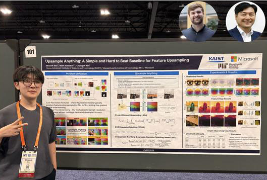
and Prof. Changick Kim (corresponding author)>
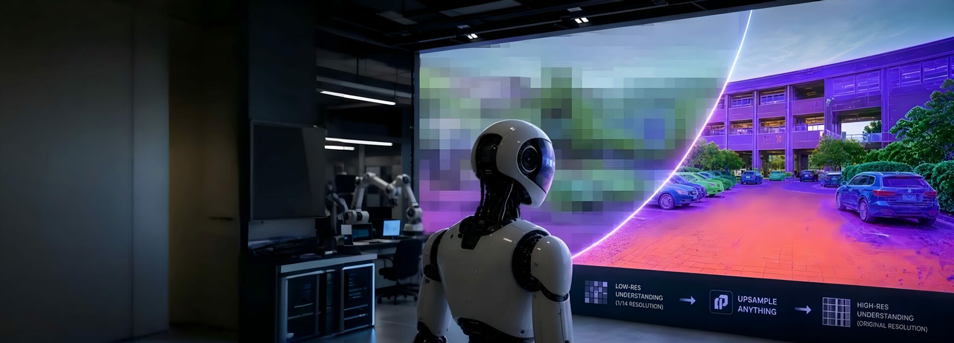
A research team led by Professor Changick Kim from EE, through joint research with researchers from MIT and Microsoft, has developed ‘Upsample Anything’—a universal technology that enhances AI vision performance even with limited GPU memory.
Submitted to CVPR 2026, the world’s most prestigious computer vision and AI conference, the paper achieved the extraordinary feat of ranking 1st overall among all 4,089 submissions.
Furthermore, in recognition of its highly efficient utilization of computational resources, the technology was awarded the ‘CVPR Compute Gold Star’—an elite distinction presented to only 18 of the submitted papers. The team was also named a ‘Transparency Champion’ for its outstanding contributions to research transparency and reproducibility.
This sweeping success widely recognizes the core elements of responsible AI research, encompassing not only raw performance but also computational efficiency, open-source code disclosure, and experimental reproducibility.

Recently, humanoid robots, autonomous driving systems, and AI based on world models (AI models that learn and predict the physical environment and changes of the real world) have been compressing input images into low-resolution features (core information extracted from images by AI) to increase computational speed and reduce memory usage.
However, during the compression process, a problem occurs where important visual information, such as small objects, thin structures, and minute defects, is lost. Conversely, processing all images at high resolution from the beginning requires massive GPU memory and computational resources, making real-time processing difficult. This has remained an unresolved challenge for a long time in situations where small devices like smartphones or robots, where mobility is crucial, must precisely perceive their surrounding environment.
To overcome these limitations, the research team developed a training-free (requiring no additional data training) upsampling technology that restores low-resolution feature information into high resolution by utilizing the edge and structural information of the input image.
Existing technologies required a separate retraining or complex optimization process to be applied to new environments or data. In contrast, ‘Upsample Anything’ developed by the research team can find the optimal restoration method using just a single input image, allowing it to be immediately applied to various environments.
In addition, by compressing and utilizing only core information instead of storing and processing all visual information at high resolution, GPU memory usage was significantly reduced. Based on a 224×224 size image (approximately 50,000 pixels) widely used in AI research, the research team restored visual information close to the original with a short calculation of about 0.4 seconds, achieving a performance that improves GPU memory efficiency by up to 16 times.
This means that artificial intelligence can perceive its surrounding environment more precisely even with limited computational resources. Therefore, this technology is expected to be widely used in various next-generation artificial intelligence fields, such as small devices like smartphones, as well as humanoid robots that need to accurately identify and manipulate small objects, autonomous driving systems, and on-device AI.
Professor Changick Kim said, “This technology is an algorithm that can significantly increase the visual precision of artificial intelligence with fewer resources, and it is expected to accelerate the commercialization of humanoid robots and on-device AI.” He added, “It is even more meaningful because it was recognized at CVPR not only for its performance but also for its computational efficiency and research transparency.”
This research was participated in by KAIST PhD student Minseok Seo as the first author, and this achievement was presented on June 7 at ‘CVPR 2026,’ the world’s most prestigious conference in the field of artificial intelligence and computer vision.
- Paper Title: Upsample Anything: A Simple and Hard to Beat Baseline for Feature Upsampling
- DOI:10.48550/arXiv.2511.16301
- Author Information: Minseok Seo (First Author), Mark Hamilton (MIT, Microsoft, Second Author), Changick Kim (Corresponding Author)


As the global semiconductor industry enters the so-called “2 nm (nanometer, one-billionth of a meter) process” era, the actual size of transistors — the core components of semiconductor chips — still remains above 10 nm. How much smaller, then, can transistors actually get? KAIST researchers have developed a technology to predict that limit through quantum mechanical atom-level calculations.
A research team led by Professor Yong-Hoon Kim of EE has developed a computational design technology that utilizes computer simulations to analyze and predict the scaling limits of transistors, a key challenge in developing next-generation semiconductor devices.
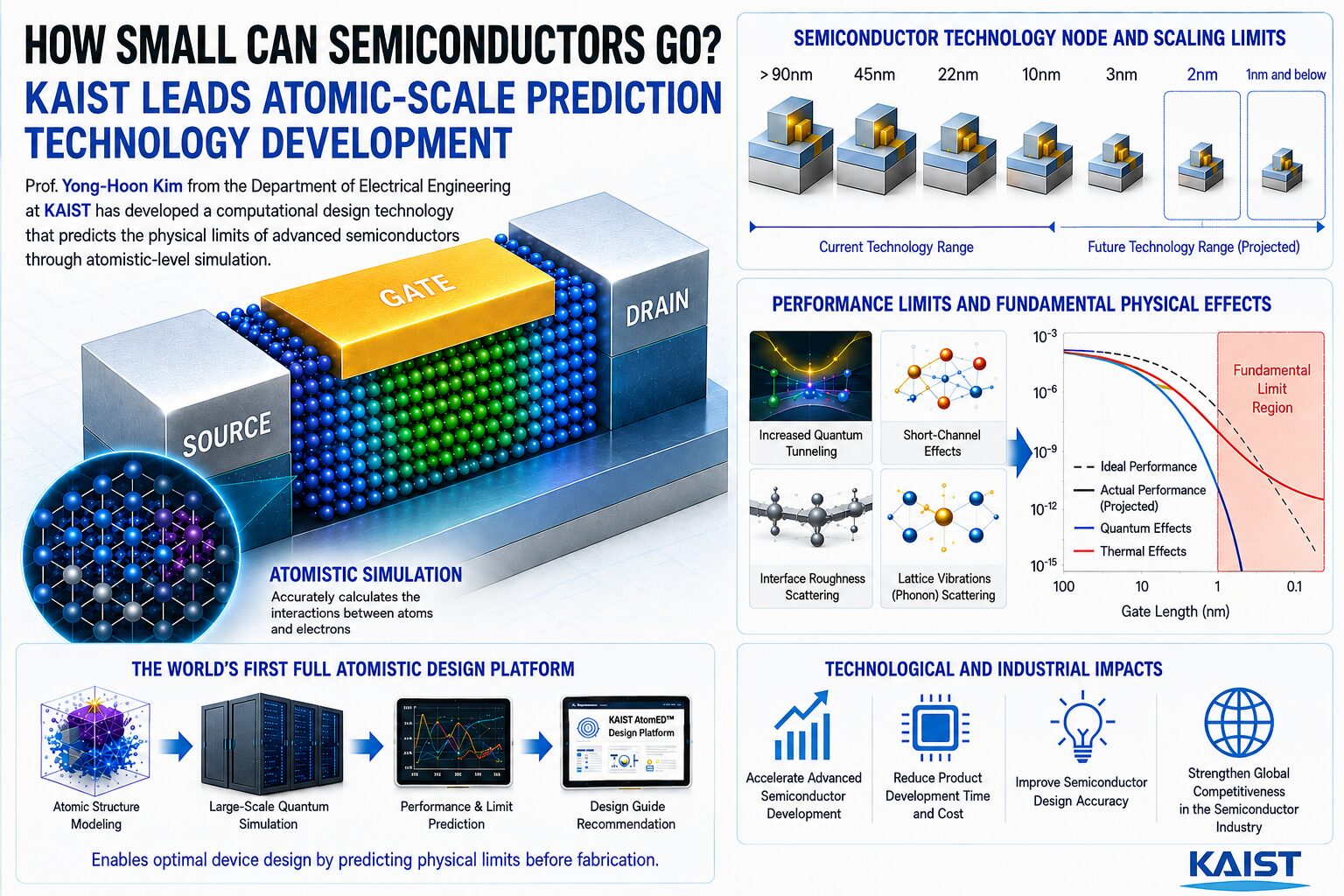
Transistors are ultra-small switches that turn electrical currents on and off, serving as key components that determine the performance and power efficiency of semiconductor chips that power smartphones, artificial intelligence computers, and more. The semiconductor industry has continuously downsized transistors to achieve higher performance and lower power consumption. However, when the size becomes excessively small, quantum tunneling occurs—a quantum mechanical phenomenon where electrons pass through energy barriers they normally cannot cross—making current control difficult. For this reason, identifying how much smaller transistors can be made within the boundaries of quantum tunneling is a critical task in next-generation semiconductor development.
However, it is virtually impossible to experimentally confirm the scaling limits of transistors directly. With current technology, it is difficult to precisely control and quantitatively analyze the contact area where the metal electrode and the semiconductor channel (the pathway through which current flows inside a transistor) meet at the atomic level.
The research team resolved this issue by utilizing ab initio or first-principles calculations, a method that computes material properties based solely on fundamental physics laws without relying on experimental data. The research team had previously developed and reported a new theoretical-computational framework called multi-space constrained-search density functional theory (MS-DFT), which extends the scope of first-principles calculations from materials to devices by precisely analyzing the complex quantum phenomena occurring at the interface where metal electrodes and semiconductors meet and across which electrons flow.
In this study, the team built on this framework to perform computational transfer length method (TLM) experiments, the gold standard experimental technique for extracting contact resistance (the resistance to current flow occurring at the metal electrode-semiconductor interface). Based on the atomic-level TLM calculations results, they identified the quantum tunneling limit (the length at which electrons stop leaking and begin to allow transistor current control).
The research team applied this technology to a monolayer MoS₂ (molybdenum disulfide) device, a representative two-dimensional semiconductor material that can be made as thin as an atomic layer and is a candidate material for next-generation transistor channels. As a result, they were able to quantitatively analyze how deeply electrons penetrate into the channel and how much this hinders current flow control depending on the type of metal electrode and the contact atomic geometry. In other words, they clarified that the limit to how small a transistor can be made varies depending on which metal and contact structure are selected. This implies that the performance and limits of a device can now be predicted in advance solely through computer simulations before the actual transistor fabrication.
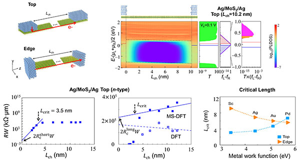
According to the research results, the critical tunneling length—the maximum length at which electrons penetrate into the channel and begin to affect transistor operation—was found not to be a single fixed value. This length emerged as a design variable that changes depending on the work function of the metal (the minimum energy required to remove an electron from a metal) and the contact structure of the interface where the metal and semiconductor meet. This signifies that the extent to which a transistor can be downsized depends on the combination of materials and structural design.
In particular, among the candidate metal types and contact structures considered, the research team confirmed that the length where electrons stop leaking could be reduced to less than 4 nm. This result demonstrates the possibility of making transistors even smaller than the levels achieved today.
Furthermore, the research team proposed a design strategy for next-generation semiconductor chips that reduce power consumption by combining two-dimensional semiconductors with different properties.
This study is significant because it establishes a platform for predicting scaling limits and designing optimal device configurations before actually fabricating semiconductor chips. Through this, it is expected to reduce trial and error and shorten the development period in the process of developing next-generation ultra-small AI semiconductor devices.
Professor Yong-Hoon Kim said, “This study is significant because it presents a new physical criterion for defining how small next-generation transistors can become. By computationally analyzing quantum mechanical phenomena in the sub-10 nm regime, which are difficult to probe experimentally, we have opened a path toward utilizing these findings in next-generation transistor design.”
The study, in which Dr. Tae Hyung Kim participated as the first author, was published online on May 28th in the prestigious computational journal ‘npj Computational Materials, a prestigious journal in the field of computational materials science
- Title of the paper: Ab initio transfer length method simulations of tunneling limits in 2D semiconductors
- DOI: https://doi.org/10.1038/s41524-026-02101-1
This research was conducted with support from programs such as the Mid-Career Researcher Program and EDISON 2.0 Program of the National Research Foundation of Korea.


Two research teams from KAIST EE have claimed first place in international challenge competitions held at the world’s premier robotics and computer vision conferences.
The ACDC-K Team and the Curaytor Team, both from the laboratory of Prof. Hyun Myung, won first place in international challenge competitions held in conjunction with the IEEE International Conference on Robotics and Automation (ICRA 2026) and the IEEE/CVF Conference on Computer Vision and Pattern Recognition (CVPR 2026), respectively.
The achievement highlights the global competitiveness of KAIST’s robotic perception and spatial intelligence technologies, with two teams from the same laboratory securing victories in leading international competitions across distinct research fields.
The ACDC-K Team won first place among more than 60 participating teams in the SLAM (Simultaneous Localization And Mapping) category of the Hilti×Trimble SLAM Challenge 2026, held during the Open Challenges in Robotics for Asset Inspection (OCRAIM) Workshop at ICRA 2026 in Vienna, Austria, from June 1 to 5.

Jointly organized by Hilti, Trimble, and the University of Oxford, the challenge evaluates robotic localization and mapping performance using sensor data collected from real construction sites. Participants were required to address practical challenges frequently encountered in construction environments, including non-overlapping front and rear fisheye camera configurations, low-texture indoor scenes, and rapid camera motion.
To tackle these challenges, the ACDC-K Team developed a robust visual-inertial SLAM system that fuses front and rear fisheye camera data with inertial measurements. By integrating feature-point and feature-line observations with adaptive constraints and correction mechanisms, the team achieved highly reliable localization and mapping performance in complex construction environments.

Meanwhile, the Curaytor Team won first place among eight participating teams in the Nothing Stands Still (NSS) Challenge 2026, held during the Computer Vision for the Built World (CV4AEC) Workshop at CVPR 2026 in Denver, Colorado, from June 3 to 7.

Jointly organized by Stanford University, ETH Zurich, and Oregon State University, the NSS Challenge evaluates 3D point cloud registration technologies for construction and industrial environments that evolve over time.
The Curaytor Team developed a novel multi-registration framework capable of aligning multiple LiDAR scans collected across different times and locations. The framework integrates feature extraction, correspondence estimation, robust global registration, registration confidence assessment, and change-aware refinement techniques. As a result, the team achieved highly accurate registration performance even in environments containing structural changes and dynamic objects.

“This achievement demonstrates the robustness of our visual-inertial SLAM and 3D LiDAR registration technologies in complex and constantly changing real-world environments,” said Prof. Hyun Myung. “It is particularly meaningful that our students secured first-place finishes in highly competitive international challenges hosted at two of the world’s most prestigious conferences in robotics and computer vision.”
Prof. Hyun Myung’s laboratory has consistently demonstrated excellence in spatial intelligence research. The laboratory previously won first place in the LiDAR track and ranked first among academic teams in the vision track of the Hilti SLAM Challenge in 2023. In addition, the Curaytor Team successfully defended its title in the NSS Challenge, securing back-to-back championships in 2025 and 2026.