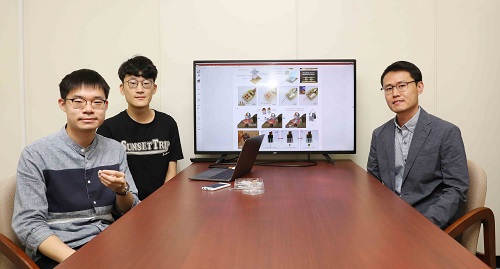
Professor Hyun-Joo Lee was reported in Etnews for ML based approach to Alzheimer's

Professor Hyun-Joo Lee was reported in Etnews 18th June for her machine learning based approach to alzheimer’s.

Introduced approach first trains system using machine learning technique on EEG dataset(electrical activity in brain)

and then trained system is used to stimulate patient’s brain to cure and alleviate symptoms by removing plaques amyloïd

-which is known to cause alzheimer’s.

News link http://www.etnews.com/20170616000183 KAIST, AI,IoT based approach to alzheimer’s 

Large-Scale, Low-Power Nonvolatile Memory Based on Few-Layer MoS2 and Ultrathin Polymer Dielectrics

A research article authored by Sang Cheol Yang (KAIST EE), Junhwan Choi (KAIST CBE), Byung Chul Jang (KAIST EE), Woonggi Hong (KAIST EE), Gi Woong Shim (KAIST EE), Sang Yoon Yang (KAIST EE), Sung Gap Im (KAIST CBE), and Sung‐Yool Choi (KAIST EE; Corresponding author) was published in Advanced Electronic Materials (2019.05)

Article title: Large-Scale, Low-Power Nonvolatile Memory Based on Few-Layer MoS2 and Ultrathin Polymer Dielectrics

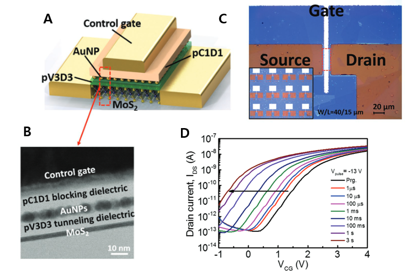
With the advent of artificial intelligence and the Internet of Things, demand has grown for flexible, low-power, high-density nonvolatile memory capable of handling vast amounts of information. Ultrathin-layered 2D semiconductor materials such as molybdenum disulfide (MoS2) have considerable potential for flexible electronic device applications because of their unique physical properties. However, development of flexible MoS2-based flash memory is challenging, as there is a lack of flexible dielectric materials with sufficient insulating properties for use in flash memory devices with dielectric bilayers. Here, large-scale, low-power nonvolatile memory is realized based on a chemical vapor deposition (CVD)-grown millimeter-scale few-layer MoS2 semiconductor channel and polymer dielectrics prepared via an initiated CVD (iCVD) process. Using the outstanding insulating properties and solvent-free nature of iCVD, fabricated memory devices with a tunable memory window, a high on/off ratio (≈106), low operating voltages (≈13 V), stable retention times exceeding 105 s with a possible extrapolated duration of years, and cycling endurance exceeding 1500 cycles are demonstrated. Owing to these characteristics, these devices distinctly outperform previously reported MoS2-based memory devices. Leveraging the inherent mechanical flexibility of both ultrathin polymer dielectrics and MoS2, this work is a step toward realization of large-scale, low-power, flexible MoS2-based flash memory.

%ED%8F%B4%EB%A6%AC%EB%A8%B8

Figure 1. A Schematic illustration of fabricated MoS2-based memory device composed of pV3D3 tunneling dielectric, Au nanoparticle (NP) FG, and pC1D1 blocking dielectric layer. B Cross-sectional HRTEM image of memory device. C Optical microscopy image of fabricated 5 × 6 memory device array. D Transfer curves as functions of pulse width during erasing operation.

Professor Sung-Yool Choi‘s research group develops a memristor-based artificial synapse for the neuromorphic chips

Prof. Sung-Yool Choi was reported in Dongascience, and 23 media, about a synapse of a neuromorphic chip implemented by memristor on February 10th.

In this research, a synaptic device in neuromorphic chips was proposed by changing the switching mechanism of the memristor device from digital to analog behavior.

The study was published in the February 2019 issue of the international journal “Nano Letters.” (Impact factor 2018 : 12.279)

Media: ‘KAIST researchers implement neuromorphic chip synapse’

http://dongascience.donga.com/news/view/26734

KIAST News: ‘KAIST Develops Analog Memristive Synapses for Neuromorphic Chips’

https://www.kaist.ac.kr/_prog/_board/?mode=V&no=93101&code=ed_news&site_dvs_cd=en&menu_dvs_cd=0601&list_typ=B&skey=&sval=&smonth=&site_dvs=&GotoPage=2


Article title: Polymer Analog Memristive Synapse with Atomic-Scale Conductive Filament for Flexible Neuromorphic Computing System

A research article authored by Byung Chul Jang (KAIST EE), Sungkyu Kim (Northwestern U), Sang Yoon Yang (KAIST EE), Jihun Park (KAIST EE), Jun-Hwe Cha (KAIST EE), Jungyeop Oh (KAIST EE), Junhwan Choi (KAIST CBE), Sung Gap Im (KAIST CBE), Vinayak P. Dravid (Northwestern U) and Sung-Yool Choi (KAIST EE; Corresponding author) was published in Nano Letters (2019.02)

The AI system leads to several issues such as limited computing power and high power consumption, making it very challenging to apply it to battery-powered mobile electronics with limited battery capacity. High power consumption of current computing hardware in the software-based implementation of artificial neural network (ANN) is mainly due to the von Neumann architecture, which is energy-inefficient for data-intensive tasks. To overcome these issues, hardware-based ANNs known as brain-inspired neuromorphic systems have been in the spotlight because the neuromorphic system can potentially emulate massively parallel networks of the biological brain with minimal energy consumption.

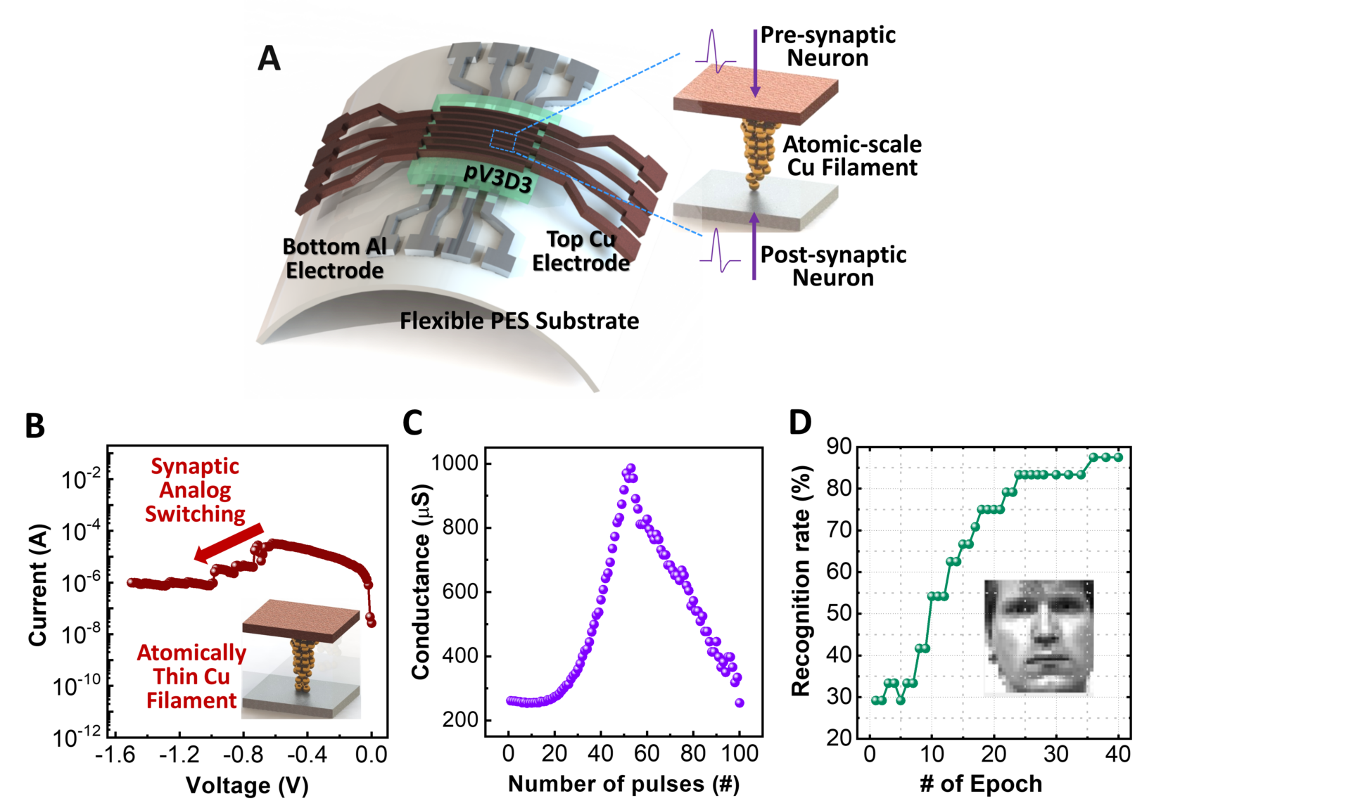
We demonstrate that flexible memristors with polymer switching layer called pV3D3 can be operated as an electronic synapse device featuring analog conductance updates simply by tuning the lateral size of the conducting filament. Reduction of the lateral size of the filament, that is, the formation of atomically thin Cu filament, resulted in the transition of switching behavior of pV3D3 memristors from abrupt to gradual mode. A linear potentiation-depression characteristic was obtained in this device, suggesting that conductance state can be updated effectively in an analog fashion when consecutive pulses are applied. Device-to-system level simulation of the face recognition also showed that the ANN based on pV3D3 memristors having atomically thin filament well classified the face images even when they were damaged.

%EB%89%B4%EB%A1%9C%EB%AA%A8%ED%94%BD%20%EC%B9%A9%20%EB%B0%8F%20%EC%8B%9C%EB%83%85%EC%8A%A4

Figure 1. A Schematic illustration of flexible pV3D3 memristor synapse array. B Analog switching behavior of polymer memristor. (Inset) Device structure of a memristor with the formation of atomically thin Cu filament. C Potentiation-depression characteristics of pV3D3 memristor. D Recognition rate of ANN for the face classification.

A Recoverable Synapse Device Using a Three-Dimensional Silicon Transistor

A research article authored by Jae Hur (KAIST EE), Byung Chul Jang (KAIST EE), Jihun Park (KAIST EE), Dong-Il Moon (KAIST EE), Hagyoul Bae (KAIST EE), Jun-Young Park (KAIST EE), Gun-Hee Kim (KAIST EE), Seung-Bae Jeon (KAIST EE), Myungsoo Seo (KAIST EE), Sungho Kim (KAIST EE), Sung-Yool Choi (KAIST EE; Corresponding author), and Yang-Kyu Choi (KAIST EE; Corresponding author) was published at Advanced Functional Materials (2018.11)

Article title: A Recoverable Synapse Device Using a Three-Dimensional Silicon Transistor

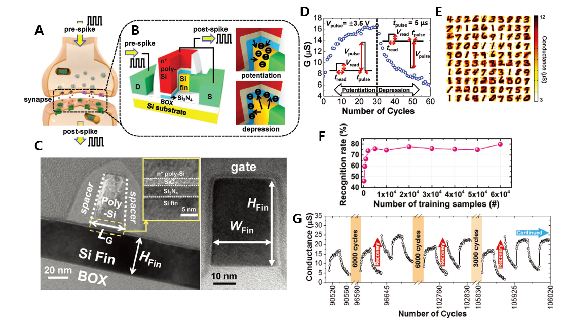
To prepare for the upcoming big-data era, numerous attempts are underway to develop a neuromorphic system which is capable of imitating a biologic neural network. Despite the significant improvements to software-based artificial neural networks (ANNs) recently, they remain inefficient in terms of energy use. Alternatively, many researchers have been attracted to hardware-based ANNs by fundamentally mimicking neural circuits and synapses. In this study, a two-terminal silicon-channel synapse (SINAPSE) with a poly-Si/SiO2/Si3N4 gate stack over a silicon channel is introduced, and demonstrated the smallest size of a synapse device reported thus far, along with reliable, low-power performance. A distinctive feature of SINAPSE is that it emulates synaptic recovery, a retrieval process for neurotransmitters which would be otherwise depleted. By applying an electrical recovery pulse to SINAPSE, synaptic recovery was for the first time successfully imitated. Experimental results demonstrate the potential of the curable SINAPSE as a fundamental unit in neuromorphic circuitry.

%ED%9A%8C%EB%B3%B5%EA%B0%80%EB%8A%A5%20%EC%8B%9C%EB%83%85%EC%8A%A4

Figure 1. A A schematic illustration of a synapse between a presynaptic and postsynaptic neuron in a biological system. B A schematic of the SINAPSE structure and the electron trajectories during the potentiation and depression processes of the charge-trap nitride of SINAPSE. C Cross-sectional TEM images of SINAPSE along the silicon nanowire direction (left-side panel) and along the gate direction (right-side panel). D Analog conductance modulation behavior of SINAPSE as a function of the number of applied pulse cycles. (Inset) Applied presynaptic voltage schemes for potentiation and depression. E Learned weights map with the ANN, which is based on a SINAPSE device with 100 output neurons. F Recognition rate as a function of the number of the number of training instances. G Recovery (Vpulse = 6 V and tpulse = 1 ms) results for SINAPSE after fatigue.

Professor Jae-Woong Jeong's research team developed a wireless control technology of the neural network in the brain using a smartphone

Through cooperative research of Professor Jae-Woong Jeong in our department and Michael Bruchas in University of Washington, their research team developed a wireless device for brain implantation which can control neural network precisely. The precise control is enabled by drug infusion and light emission to particular areas of the brain. This technology is expected to be applied not only to the development of new drugs which needs animal testing but also to the treatment of a brain disorder such as Parkinson’s.

The research, for which Raza Qazi (first author of the paper), Choong Yeon Kim, and Sang Hyuk Byun developed the device and in which neural science research team from University of Washington collaborated, was published in Nature Biomedical Engineering on 6th, August (The title of the paper: Wireless optofluidic brain probes for chronic neuropharmacology and photostimulation). By optogenetics and neuropharmacology, target neurons or neural circuits can be controlled without affecting other neural circuits. Because it has a much finer spatiotemporal resolution than conventional electrostimulation, this method is recently focused on the purpose of brain research and treatment of brain disorders.

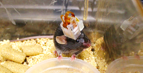
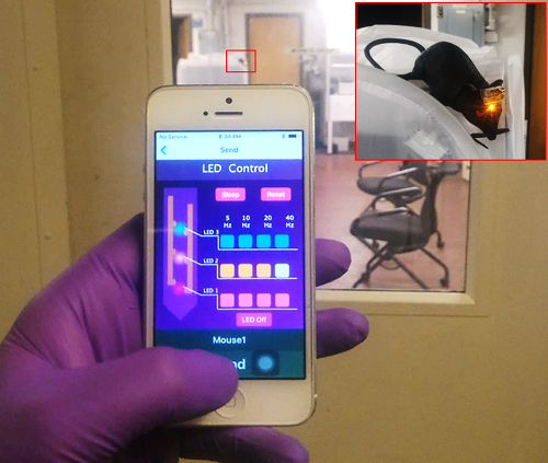
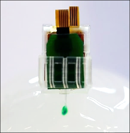
However, current devices which are mostly used for brain research are some problems; damage to brain structure and their inability to control brain circuits precisely and be designed as one multifunctional probe. Also, there is a gap between soft brain structure and hard materials like silica and metal which are constitutive of the devices. With these reasons, those devices will aggravate infections so they are not appropriate to be implanted for a long time. The research team made tiny flexible probes by combining microfluidic probes and micro LEDs and fused the probes with small control circuits based on Bluetooth and replaceable drug cartridges. Thus, the team invented the neural-implantable device with a smartphone Bluetooth control of LED and drug infusion. Especially, the drug cartridges were designed to imitate LEGO so new cartridges can be connected to the device to provide drugs repetitively for a long time. Research team implanted the device on a target neural circuit of a mouse and combined cartridges with dopamine activator and inhibitor. Finally, the team succeeded in activating and inhibiting the behavior of the mouse by using the smartphone application.

In addition, the research team injected light-sensitive protein into the brain of a mouse to stimulate place preference. The team made the mouse prefer particular place by turning on the micro-LED when the mouse moved to the place. In contrast, the team successfully deleted place preference of the mouse using drugs. Professor Jae-Woong Jeong said, “nerve control using light and drug is more exquisite and this makes it possible to control the brain without side effects. The invented device needs the easy smartphone operation to control specific brain circuits using light and drugs repetitively and continually. Therefore, the device will be adapted to studies of brain functions and treatments of brain disorders.”

The research team is studying to improve the device to apply this technology to human by implanting the device in the human skull completely and perpetually.


Figure 1. Mouse with implanted control device                                               Figure 2. Micro LED control by a smartphone app

%EB%94%94%EB%B0%94%EC%9D%B4%EC%8A%A4%EA%B0%80%20%EC%9D%B4%EC%8B%9D%EB%90%9C%20%EC%A5%90%EC%9D%98%20%EC%82%AC%EC%A7%84 %EC%8A%A4%EB%A7%88%ED%8A%B8%ED%8F%B0%EC%95%B1%EC%9D%84%20%EC%9D%B4%EC%9A%A9%ED%95%9C%20%EB%A7%88%EC%9D%B4%ED%81%AC%EB%A1%9C%20LED%20%EC%BB%A8%ED%8A%B8%EB%A1%A4 0

Figure 3. Developed wireless brain-implantable device

%EA%B0%9C%EB%B0%9C%EB%90%9C%20%EB%87%8C%20%EC%9D%B4%EC%8B%9D%EC%9A%A9%20%EB%AC%B4%EC%84%A0%20%EB%94%94%EB%B0%94%EC%9D%B4%EC%8A%A4

Professors Sung-Yool Choi & Sang-Hee Ko Park’s research group implements the low-power (1S-1R) logic-in-memory integrated circuit

Prof. Sung-Yool Choi & Sang-Hee Ko Park’s research group were reported in Yonhapnews, and 14 media, about implementing low-power memristor integrated circuit on February 13th, 2018.

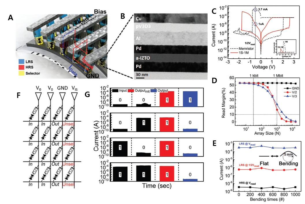
This research is to provide a low-power nonvolatile flexible logic-in-memory circuit that suppresses sneak current and leakage current by integrating (1S-1M) memristors and selector devices.

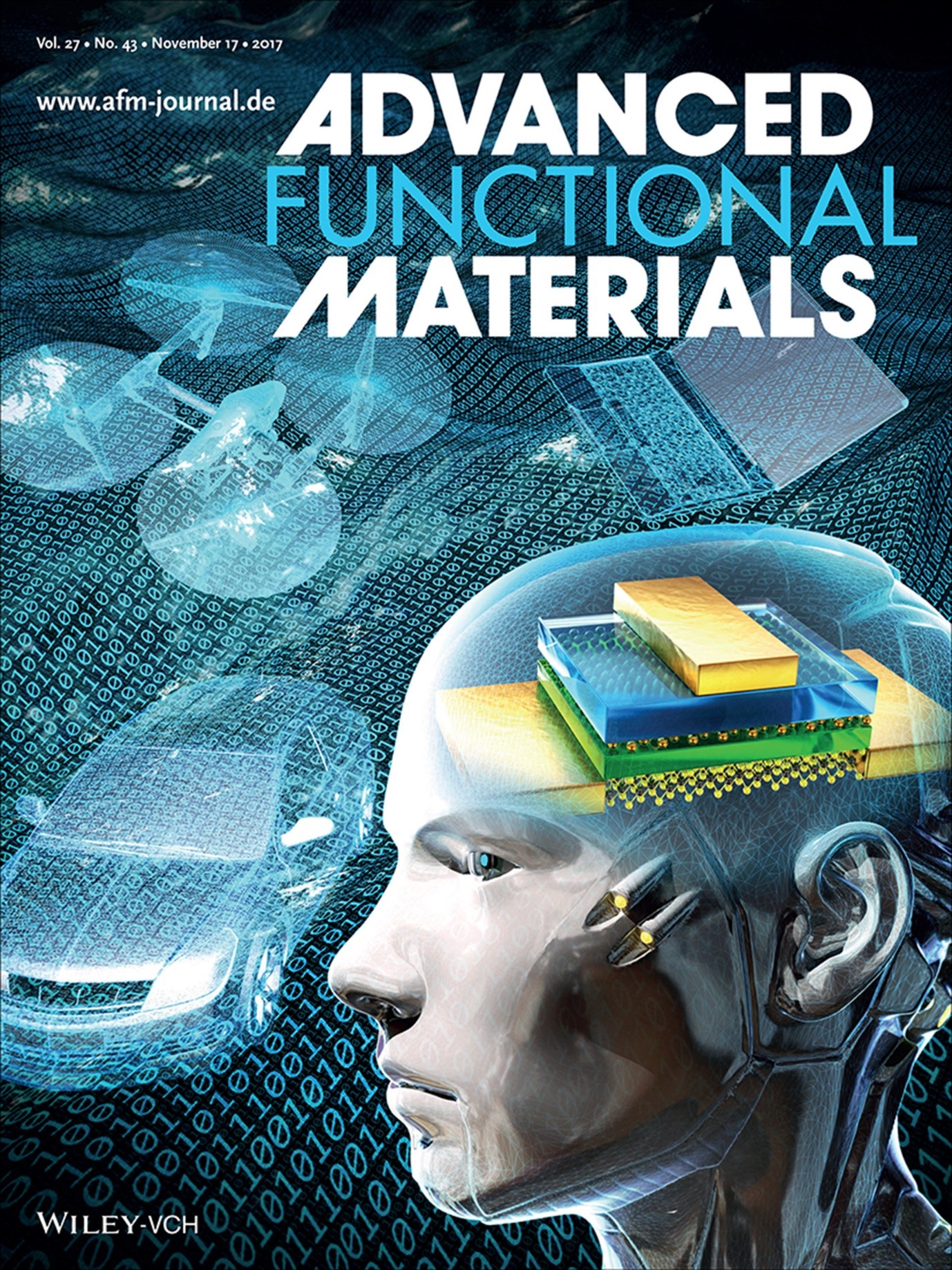
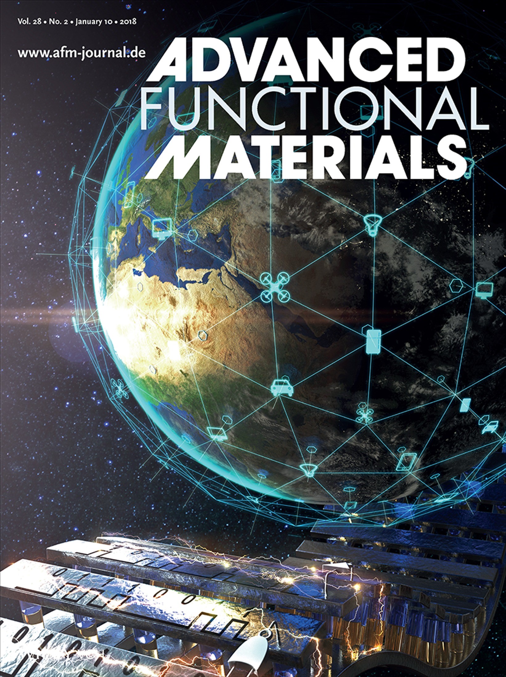
The study was published as a cover paper in January 2018 in the international journal ‘Advanced Functional Materials’. (Impact factor 2018 : 13.325)

Media: ‘KAIST, memristor integrated circuit development to reduce power consumption‘

https://www.yna.co.kr/view/AKR20180213103900063?input=1195m

KAIST News: ‘Low-power, Flexible Memristor Circuit for Mobile and Wearable Devices’

https://www.kaist.ac.kr/_prog/_board/?mode=V&no=77021&code=ed_news&site_dvs_cd=en&menu_dvs_cd=0601&list_typ=B&skey=&sval=&smonth=&site_dvs=&GotoPage=9

KAIST EE: ‘Professor Choi Sung-Yool’s team published a cover paper on Advanced Funtional Materials’

https://ee.kaist.ac.kr/en/research-achieve/15609/


Article title: Memristive Logic‐in‐Memory Integrated Circuits for Energy‐Efficient Flexible Electronics

A research article authored by Byung Chul Jang (KAIST EE), Yunyong Nam (KAIST MSE), Beom Jun Koo (KAIST EE), Junhwan Choi (KAIST CBE), Sung Gap Im (KAIST CBE), Sang‐Hee Ko Park (KAIST MSE; Corresponding author), and Sung‐Yool Choi (KAIST EE; Corresponding author) was published at Advanced Functional Materials (2018.01)

The use of von Neumann architecture, with its physically separate memory and processor, generates an extremely large energy-hungry data transfer between the memory and processor, inducing long latency and high power consumption. The memristor has been proposed as the fourth fundamental circuit element and can provide a creative solution to these problems. The memristor device has been widely investigated for a promising nonvolatile memory due to its simple structure, fast switching speed, low power consumption, and high packing density. The crossbar array is the optimal architecture enabling high packing density, defect tolerance, and logic operation; however, this architecture generates an inherent cell-to-cell interference problem. As this interference allows undesirable leakage currents known as “sneak currents” to flow through unselected devices during memristor operations, it limits the maximum array size and prevents the memristive nonvolatile logic-in-memory circuit from enabling parallel computing.

Herein, we develop a 1S–1M integrated circuit using a poly (1,3,5-trivinyl-1,3,5-trimethyl cyclotrisiloxane) (pV3D3)-based memristor and an a-IZTO-based selector on a flexible polyethersulfone (PES) substrate to propose a conceptual strategy for realizing an energy-efficient memristive nonvolatile logic-in-memory circuit, enabling parallel computing. The fabricated flexible a-IZTO-selector device exhibits outstanding stability against harsh electrical stress and mechanical strain. Using X-ray photoelectron spectroscopy (XPS) analysis and examining the I–V characteristics, effective removal of the a-IZTO SEAL via oxygen plasma treatment is confirmed. Thanks to this reliable and flexible a-IZTO selector, the 1S–1M integrated devices exhibit a significantly reduced leakage current under a low-voltage region compared to a 1M device, along with reliable switching performance against electrical and mechanical stresses. The reading margin of the 1S–1M array is evaluated under various operational schemes (ground, V/2, V/3), indicating a feasible maximum array size of more than 1 Mbit. We also experimentally demonstrate that the fabricated 1S–1M array can perform single-instruction multiple-data (SIMD), the basis of parallel computing, without interruption by the sneak current. We strongly believe that the proposed parallel computing method using a memristive nonvolatile logic-in-memory circuit can provide a low-power circuit platform for battery-powered flexible electronic systems with various potential applications.

%EC%B5%9C%EC%84%B1%EC%9C%A8%2C%20%EB%B0%95%EC%83%81%ED%9D%AC%20%EA%B5%90%EC%88%98%EB%8B%98%20%EC%9E%90%EB%A3%8C

Figure 1. A Schematic illustration of integrated selector device role in memristor crossbar array during operation. B Cross-sectional TEM image of 1S–1M device. C Comparison of I–V characteristics of 1S–1M and 1M devices. Inset: Nonlinear I–V characteristics of 1S–1M device on linear scale compared with 1M device. D Calculated reading margin comparison for three reading bias schemes as function of array size. E Repetitive bending fatigue test for 1S–1M device. F Schematic of MAGIC-NOR gates within 1S–1M memristor array. G Experimental results for parallel operation of MAGIC-NOR gates.
%ED%91%9C%EC%A7%80%EC%82%AC%EC%A7%842

Prof. Sung-Yool Choi & Sung Gap Im’s research group develops ultra-low-power nonvolatile flexible memory based on two-dimensional materials

Prof. Sung-Yool Choi & Sung Gap Im’s research group were reported in Yonhapnews, and 17 media, about the nonvolatile two-dimentional memory on December 18th, 2017.
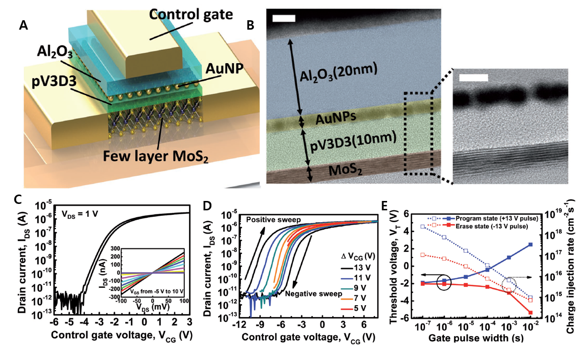
In this research, the highly integrated, ultra-low-power, and flexible nonvolatile memory was demonstrated using two-dimensional material (MoS2) and polymer insulating thinfilm.
The study was published as a cover paper in November 2017 in the international journal ‘Advanced Functional Materials’. (Impact factor 2017: 12.12)

Media: ‘KAIST, implement a ultra-low-power flexible memory‘
https://www.yna.co.kr/view/AKR20171218056900063?input=1195m 
KAIST News: ‘Ultra-Low Power Flexible Memory Using 2D Materials’
https://www.kaist.ac.kr/_prog/_board/?mode=V&no=75023&code=ed_news&site_dvs_cd=en&menu_dvs_cd=060101&list_typ=B&skey=&sval=&smonth=&site_dvs=&GotoPage=11

Article title: Low‐Power Nonvolatile Charge Storage Memory Based on MoS2 and an Ultrathin Polymer Tunneling Dielectric
A research article authored by Myung Hun Woo (KAIST EE), Byung Chul Jang (KAIST EE), Junhwan Choi (KAIST CBE), Khang June Lee (KAIST EE), Gwang Hyuk Shin (KAIST EE), Hyejeong Seong (KAIST CBE), Sung Gap Im (KAIST CBE), and Sung‐Yool Choi (KAIST EE; Corresponding author) was published at Advanced Functional Materials (2017.11)

Low-power, nonvolatile memory is an essential electronic component to store and process the unprecedented data flood arising from the oncoming Internet of Things era. Molybdenum disulfide (MoS2) is a 2D material that is increasingly regarded as a promising semiconductor material in electronic device applications because of its unique physical characteristics. However, dielectric formation of an ultrathin low-k tunneling on the dangling bond-free surface of MoS2 is a challenging task. Here, MoS2-based low-power nonvolatile charge storage memory devices are reported with a poly(1,3,5-trimethyl- 1,3,5-trivinyl cyclotrisiloxane) (pV3D3) tunneling dielectric layer formed via a solvent-free initiated chemical vapor deposition (iCVD) process. The surface-growing polymerization and low-temperature nature of the iCVD process enable the conformal growing of low-k (≈2.2) pV3D3 insulating films on MoS2. The fabricated memory devices exhibit a tunable memory window with high on/off ratio (≈106), excellent retention times of 105 s with an extrapolated time of possibly years, and an excellent cycling endurance of more than 103 cycles, which are much higher than those reported previously for MoS2-based memory devices. By leveraging the inherent flexibility of both MoS2 and polymer dielectric films, this research presents an important milestone in the development of low-power flexible nonvolatile memory devices. 

%EC%B5%9C%EC%84%B1%EC%9C%A8%20%EA%B5%90%EC%88%98%EB%8B%98%20%EC%96%B8%EB%A1%A0%EB%B3%B4%EB%8F%84 1

Figure 1. A Schematic illustration of the fabricated memory device, which is composed of a pV3D3 tunneling dielectric, AuNPs as floating gate, and an Al2O3 blocking dielectric layer. B Cross-sectional TEM image of the device. C Initial transfer characteristics of the memory device with control gate voltage. The inset shows the memory device contact properties. D Transfer characteristics with VCG sweeping in the negative-to-positive direction and back, with fixed VDS = 1 V. E Extracted threshold voltage shift for different pulse widths, and calculated charge injection rate in program and erase operations.


%ED%91%9C%EC%A7%80%20%EC%82%AC%EC%A7%84 0

Professors Yang-Kyu Choi & Sung-Yool Choi’s research group develops wearable logic in-memory circuitry on commercial fabric

Professors Yang-Kyu Choi & Sung-Yool Choi’s research group were reported in Etnews about the wearable logic-in-memory using memristor on February 10th, 2018.

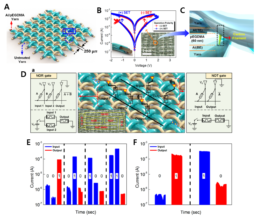
The research develops a wearable logic-in-memory based on memristors by weaving a special thread coated with electrode and polymer insulating layer.

The study was published in the October 2017 issue of the international journal “Nano Letters.” (Impact factor 2017 : 12.080)


Media: ‘KAIST, implementing storage and computation device by weaving the thread… Implementing new concept of the wearable device’

http://www.etnews.com/20180328000205

KAIST EE: ‘Research by Ph.D candidate Bae, Hak-Yeol and Jang, Byung-Cheol has been published in Nano Letters’

https://ee.kaist.ac.kr/en/research-achieve/15452/


Article title: Functional Circuitry on Commercial Fabric via Textile-Compatible Nanoscale Film Coating Process for Fibertronics

A research article authored by Hagyoul Bae (KAIST EE), Byung Chul Jang (KAIST EE), Hongkeun Park (KAIST CBE), Soo-Ho Jung (KIMS), Hye Moon Lee (KIMS), Jun-Young Park (KAIST EE), Seung-Bae Jeon (KAIST EE), Gyeongho Son (KAIST EE), Il-Woong Tcho (KAIST EE), Kyoungsik Yu (KAIST EE), Sung Gap Im (KAIST CBE), Sung-Yool Choi (KAIST EE; Corresponding author), and Yang-Kyu Choi (KAIST EE; Corresponding author) was published in Nano Letters (2017.10)

Fabric-based electronic textiles (e-textiles) are the fundamental components of wearable electronic systems, which can provide convenient hand-free access to computer and electronics applications. However, e-textile technologies presently face significant technical challenges. These challenges include difficulties of fabrication due to the delicate nature of the materials, and limited operating time, a consequence of the conventional normally on computing architecture, with volatile power-hungry electronic components, and modest battery storage. Here, we report a novel poly(ethylene glycol dimethacrylate) (pEGDMA)-textile memristive nonvolatile logic-in-memory circuit, enabling normally off computing, that can overcome those challenges. To form the metal electrode and resistive switching layer, strands of cotton yarn were coated with aluminum (Al) using a solution dip coating method, and the pEGDMA was conformally applied using an initiated chemical vapor deposition process. The intersection of two Al/pEGDMA coated yarns becomes a unit memristor in the lattice structure. The pEGDMA-Textile Memristor (ETM), a form of crossbar array, was interwoven using a grid of Al/pEGDMA coated yarns and untreated yarns. The former were employed in the active memristor and the latter suppressed cell-to-cell disturbance. We experimentally demonstrated for the first time that the basic Boolean functions, including a half adder as well as NOT, NOR, OR, AND, and NAND logic gates, are successfully implemented with the ETM crossbar array on a fabric substrate. This research may represent a breakthrough development for practical wearable and smart fibertronics.

%EC%B5%9C%EC%96%91%EA%B7%9C%20%EA%B5%90%EC%88%98%EB%8B%98%20%EC%96%B8%EB%A1%A0%EB%B3%B4%EB%8F%84 1

Figure 1. A Conceptual image of the fabricated memory device based on the cross-linked Al/pEGDMA-coated yarns. B Bipolar I−V characteristic of the fabricated ETM array on the cotton substrate with a pEGDMA film thickness of 60 nm. The inset shows the optical microscope image of the fabricated ETM array and the schematic image of the Al/pEGDMA-coated yarn. C Schematic view of the formation of a conductive carbon filament bridging of TE and BE via the pEGDMA. D Schematic of the logic-in-memory operations of NOR and NOT gates and their equivalent circuits within the crossbar array via the MAGIC architecture. The inset presents a conceptual image for integration of each logic gate on the fabric. E Experimental results of the MAGIC-NOR gate. F Experimental results of the MAGIC-NOT gate.

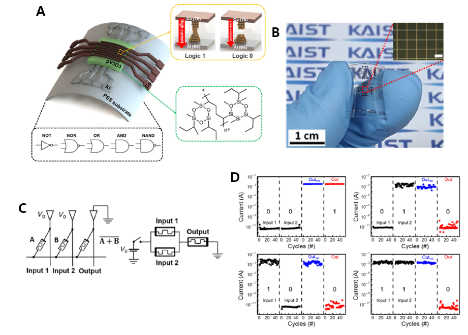
Zero-static-power nonvolatile logic-in-memory circuits for flexible electronics

A research article authored by Byung Chul Jang (KAIST EE), Sang Yoon Yang (KAIST EE), Hyejeong Seong (KAIST CBE), Sung Kyu Kim (KAIST MSE), Junhwan Choi (KAIST CBE), Sung Gap Im (KAIST CBE), and Sung-Yool Choi (KAIST EE; Corresponding author) was published at Nano Research (2017.07)

Article title: Zero-static-power nonvolatile logic-in-memory circuits for flexible electronics

Flexible logic circuits and memory with ultra-low static power consumption are in great demand for battery-powered flexible electronic systems. Here, we show that a flexible nonvolatile logic-in-memory circuit enabling normally-off computing can be implemented using a poly(1,3,5-trivinyl-1,3,5-trimethyl cyclotrisiloxane) (pV3D3)-based memristor array. Although memristive logic-in-memory circuits have been previously reported, the requirements of additional components and the large variation of memristors have limited demonstrations to simple gates within a few operation cycles on rigid substrates only. Using memristor-aided logic (MAGIC) architecture requiring only memristors and pV3D3-memristor with good uniformity on a flexible substrate, for the first time, we experimentally demonstrated our implementation of MAGIC-NOT and -NOR gates during multiple cycles and even under bent conditions. Other functions, such as OR, AND, NAND, and a half adder, are also realized by combinations of NOT and NOR gates within a crossbar array. This research advances the development of novel computing architecture with zero static power consumption for battery-powered flexible electronic systems.

Zero%20static

Figure 1. A Schematic illustration of a pV3D3-memristor with an 8 × 8 crossbar array on a plastic substrate. The inset with the orange dotted line shows the logical states of the pV3D3-memristor, the inset with the green dotted line shows the molecular structure of pV3D3, and the inset with the black dotted line depicts the feasible logic gates using the pV3D3-memristor. B Photograph of a flexible pV3D3-memristor on a PES substrate. The inset shows a magnified optical image of the flexible pV3D3-memristor array (scale bar: 20 μm). C MAGIC-NOR gate within the crossbar array and its equivalent circuit. D Experimental results of the MAGIC-NOR gate for all input memristor combinations during 50 cycles.